Atomic force microscopy has long revealed surface wonders to scientists from many disciplines. Now new probes are bringing improved resolution. Yfke Hager investigates
Atomic force microscopy has long revealed surface wonders to scientists from many disciplines. Now new probes are bringing improved resolution. Yfke Hager investigates
Two decades ago, a wave of excitement spread through the world of surface science: atomic force microscopy (AFM) had appeared on the scene. AFM is now ubiquitous in chemistry, biology and physics labs around the world, where it is used to study phenomena such as adhesion, corrosion, etching, friction and lubrication. It has also opened up new avenues of research. ’AFM is one of the key tools for nanotechnological research,’ says Julie Macpherson, a researcher in the chemistry department at the University of Warwick, UK. A keen advocate for AFM, Macpherson explains that it was first used to image the topography of surfaces. ’But then people realised that there are many other forces we can explore, like chemical and magnetic forces, so the field really exploded.’
AFM explained
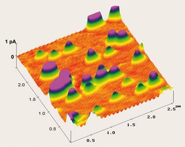
AFMs work by scanning across a sample surface with a sharp probe tip attached to a force-sensing cantilever. As the tip moves along the surface, the cantilever deflects in response to force interactions between the probe tip and the sample. Researchers monitor these deflections by shining a laser beam off the back of the cantilever into a photosensitive detector, creating a topographical map of the sample surface. But the AFM is much more than a surface-mapping tool; it also measures the force between the tip and the substrate at the nano-newton scale. The AFM has several advantages over the electron microscope: it provides a three-dimensional surface profile rather than a two-dimensional image, AFM samples do not require any special treatment before scanning, and it works in air and liquid, which is particularly important for the imaging of biological substrates under physiologically relevant conditions.
Carbon nanotubes
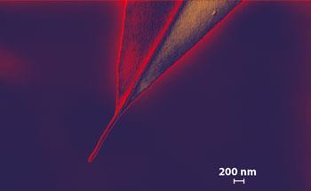
AFM may have revolutionised surface microscopy, but the technique still has its limitations. Unlike optical microscopes, AFMs do not use a lens, so AFM resolution is limited by probe size rather than diffraction effects. Typical AFM probe tips are made of silicon or silicon nitride, which provide lateral resolutions of 5-10nm and 10-40nm, respectively. ’To improve the resolution, people are trying to produce sharper tips,’ Macpherson says.
Nanotechnology inspired the first improved tips. Hongjie Dai and the late Nobel prize winner Richard Smalley at Houston’s Rice University, US, came up with the idea to attach a carbon nanotube to the end of a conventional silicon AFM probe tip. Carbon nanotube tips offer higher resolution than conventional tips for several reasons. AFM resolution depends on both the size of the probe tip and the strength of adhesive interactions between the tip and sample. Carbon nanotube probes happen to combine extremely small size with very low adhesion to the sample surface. Nanotubes are also desirable because they buckle rather than break under high loads, just like a drinking straw buckles if you squeeze it from both ends. They are also more durable than conventional probes and have a higher aspect ratio, so they can probe dips and crevices in the sample surface.
However, multi-walled carbon nanotubes, which consist of many concentric carbon shells, do not offer much better resolution than the sharpest AFM probes that are currently commercially available. Single-walled carbon nanotubes have much smaller diameters, and therefore make better tips. ’By many, [single-walled carbon nanotubes] are seen as the ultimate imaging tip,’ Macpherson says. But they are incredibly time-consuming to make, and so far nobody has come up with a reliable way to batch manufacture single-walled tubes at a reasonable cost.
Aleksandr Noy at the Lawrence Livermore National Laboratory, California, US, is reluctant to create carbon nanotube probe tips. ’When you balance the gain [in terms of improved resolution] with the effort it takes to make the tips, you need to have an application that requires such resolution to justify going through the effort of fabricating your own nanotube probes,’ he says. An obvious solution is to obtain the probes commercially, he says; a number of companies offer this high-priced possibility. But most of these probes have multi-wall nanotube tips, which are not stable in water, restricting applications for biological imaging. ’If a company could bring to the market single-wall carbon nanotube AFM probes that are stable in fluids, and do it at a price comparable to current AFM tip prices, it will revolutionise imaging at small scales,’ Noy says. ’At this point it has not happened and I know that many people are looking forward to that day,’ he adds.
At the University of Nottingham, Christopher Gibson’s team is working to improve the pick-up method. Gibson grows a ’carpet’ of carbon nanotubes, then transfers the tubes to an AFM probe tip using the pick-up method. ’We change the amplitude of oscillation of the probe until the probe tip is resting on the substrate surface. This improves the [nanotube] attachment rate and the stability of attachment, which is critical as this reduces artefacts,’ Gibson explains. Currently, he says, the Nottingham team has no plans for batch processing or commercialisation of the process.
Rising to the challenge of batch fabrication of single-walled carbon nanotubes, a collaboration has sprung up between Macpherson’s group in Warwick and Phil Dobson and John Weaver at Glasgow University, UK. ’Our collaboration draws on Warwick’s scientific expertise in growing the tubes, and our engineering expertise to manufacture the tips,’ Weaver says. The Glasgow researchers use photolithography, electron beam lithography, material etching and material deposition techniques to produce wafers of hundreds of AFM probes. They have developed a method to grow single-wall carbon nanotubes directly onto the probes in a way that maximises attachment forces. ’The method we are working on defines small regions of catalyst [iron or cobalt] on each probe tip,’ Dobson says. ’Tubes only form on regions coated in catalyst, so when tubes are grown on the wafer they will only be present at the probe tips, where they are wanted.’ This approach gives them the best of both worlds, Dobson says: mass-produced nanotubes, with control over where they are placed on the probe tip.
Droplet interactions
AFM can also be used to study dynamic interactions between deformable surfaces. Recently, Raymond Dagastine and co-workers at the University of Melbourne, Australia, used AFM to measure the interaction forces between two oil droplets in water for the first time.
To investigate the forces between emulsion droplets, the team ’tethered’ two decane droplets to an AFM cantilever and substrate, then drove the droplets together and apart at different speeds. Examining the nanoscale interactions between the droplets, Dagastine and his team found that the overall behaviour of droplet-droplet interactions is governed by deformation, static surface forces and hydrodynamic drainage. They were also able to model, and predict, how emulsion droplets interact.
The team wants to apply its enhanced understanding of emulsion stability to processing and storage situations. The research may have applications for emulsion-based products ranging from ice cream to shampoo.
R R Dagastine et al, 2006, Science, 313 , 210
Multifunctional probes
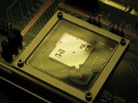
Scientists at IBM have also developed multifunctional probes. The ’Millipede’ is a data storage device that uses thousands of cantilevers with integrated microheaters to punch bits into a plastic film. In another application, an array of eight cantilevers coated with a sensor layer acts as a ’chemical nose’ to detect tiny amounts of analytes. By coating the cantilever array with different substances, the IBM team has also created pH sensors, mass sensors and calorimeters.
One AFM offshoot is a revolutionary high-density data storage device. Fondly nicknamed ’the Millipede’ by the scientists at the IBM Zurich Research Laboratory in Switzerland who developed it, the device boasts storage densities exceeding one terabit per square inch - equivalent to storing the content of 25 DVDs on an area the size of a postage stamp.
Millipede uses thousands of nanoscale tips to punch indentations representing individual bits into a thin specialised polymer film. It is essentially a nanotech version of the old-fashioned ’punch card’, but with two important differences: Millipede is
re-writeable, and stores more than 3 billion bits of data in the space occupied by one hole in a standard punch card.
At its core is a two-dimensional array of microcantilevers with extremely sharp tips. Nestled near the end of each cantilever is a heating resistor for writing, as well as a micrometre-sized sensor for reading. A micromechanical actuator moves the polymer film beneath the cantilever array. Bits are written by heating a cantilever tip to 400?C, which softens the polymer so that the tip sinks into the film, leaving an indentation only 10nm across. Data are overwritten by erasing existing pits; new pits are punched very close to the old ones, so that their edges fill in the old pits. To read data, the reading sensor is heated to a lower temperature than for writing. When the cantilever tip dips into a pit, it cools down, leading to a measurable increase in the sensor’s resistance.
The Millipede’s power consumption is well below that of magnetic recording, making it perfectly suited for use in mobile technologies. The IBM scientists hope that the technology will find its way into future mobile phones, personal organisers, digital cameras and USB memory sticks.
However, to make Millipede a commercial reality, IBM needs to find an industrial partner with expertise in the manufacture of microelectromechanical systems, so it is uncertain when the technology will make a commercial appearance.
Microscopic data storage with Millipede
One AFM offshoot is a revolutionary high-density data storage device. Fondly nicknamed ’the Millipede’ by the scientists at the IBM Zurich Research Laboratory in Switzerland who developed it, the device boasts storage densities exceeding one terabit per square inch - equivalent to storing the content of 25 DVDs on an area the size of a postage stamp.
At its core is a two-dimensional array of microcantilevers with extremely sharp tips. Nestled near the end of each cantilever is a heating resistor for writing, as well as a micrometre-sized sensor for reading. A micromechanical actuator moves the polymer film beneath the cantilever array. Bits are written by heating a cantilever tip to 400?C, which softens the polymer so that the tip sinks into the film, leaving an indentation only 10nm across. Data are overwritten by erasing existing pits; new pits are punched very close to the old ones, so that their edges fill in the old pits. To read data, the reading sensor is heated to a lower temperature than for writing. When the cantilever tip dips into a pit, it cools down, leading to a measurable increase in the sensor’s resistance.
The Millipede’s power consumption is well below that of magnetic recording, making it perfectly suited for use in mobile technologies. The IBM scientists hope that the technology will find its way into future mobile phones, personal organisers, digital cameras and USB memory sticks.
However, to make Millipede a commercial reality, IBM needs to find an industrial partner with expertise in the manufacture of microelectromechanical systems, so it is uncertain when the technology will make a commercial appearance.
Chemical force microscopy
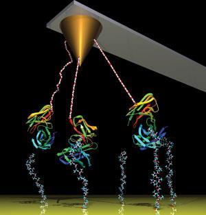
Another key development is the ability to measure forces between single molecules. Noy became interested in measuring chemical forces using AFM techniques while doing graduate work in Lieber’s lab at Harvard. ’AFM provides a unique opportunity to probe the strength of individual bonds; you can grab the bond by its ends and pull it apart,’ he explains. Recently, Noy used an AFM to probe interactions between a cancer drug and its target on a cell surface. ’We attached the drug to an AFM tip and used the tip to measure the force that it takes to pull the drug off its target.’
At Molecular Profiles, a spin-out company of Nottingham University, Shellie Rigby-Singleton also uses AFM for pharmaceutical applications. She measures adhesion and cohesion forces between particles to predict how drug molecules interact with each other, and to determine how well a drug can be processed. ’Our work with AFM helps the drug development team to know more about the properties of drug candidates in the early screening stages of drug development,’ Rigby-Singleton says. She would love to be able to measure real-time biological interactions, but AFM imaging speeds aren’t fast enough yet. ’If we can get high-speed AFM to work in a liquid substrate, that would be a really nice addition to our abilities,’ she enthuses.
High-speed AFM
Paul Hansma’s lab at the University of California, Santa Barbara, US, may soon be able to offer just that. AFM is a popular choice for biologists, as it allows imaging under physiological conditions. But ’it can take several minutes to scan at high resolution, so you cannot see things in real time,’ says Georg Schitter, a postdoc in Hansma’s group who is working on high-speed AFM. ’The reason AFM is currently so slow is that all the components are matched to each other, so you have to redesign them all to get it to work faster,’ he explains. The Hansma group has optimised the scanner’s speed performance, making it compact and rigid to achieve higher resonance frequencies. They have also shrunk the cantilever, giving a faster response. Schitter has already achieved 60 frames per second, which is almost 1000 times faster than a conventional AFM.
With these developments on the horizon, it’s likely that even more scientists and engineers will soon embrace AFM.
Yfke Hager is a science writer based in Manchester, UK.
Companies
Infinitesima, Oxford, UK, was born out of research at the University of Bristol, UK, in 2001. It specialises in developing accessories and products based on scanning probe microscopy methods and techniques. Its video atomic force microscope (AFM) delivers real-time images at video frame rates.
Agilent AFM, based in Arizona, US, develops and supplies tools for scanning probe microscopy (SPM) and AFM. These include systems, accessories, software and data management for imaging in fluids and under controlled temperature and environmental conditions. The AFM business has built up from Agilent’s acquisition of US firm Molecular Imaging Corporation in 2005.
Windsor Scientific, UK, provides a range of scanning probe microscopes and accessories. Its iprobe can measure real time surface morphology and electrochemical behaviour on a sample, using a probe acting simultaneously as a cantilever and a working electrode.
Molecular Profiles, UK, a spin-out from Nottingham University, UK, is a contract research company that deals with the pharmaceutical and healthcare industry. It offers a range of high resolution imaging services, including AFM.
Novascan, US, specialises in AFM. It sells high performance AFMs as well as custom designed AFMs integrated with a variety of complementary instruments. Novascan also offers a range of AFM tips and functionalised AFM probes.
Veeco, based in New York, US, claims to provide ’solutions for a nanoscale world’. The company mainly deals with the data storage and semiconductor industries and sells a range of scanning probe products. including AFMs.
No comments yet