Andy Extance goggles at the display revolution, the culmination of 30 years of research into organic light emitting diodes

Gown-clad students smile, posing for photos. It is part of a life-defining moment for them, but it is also one that recently brought the University of Michigan’s Stephen Forrest’s career achievements into focus. He saw two women taking pictures of a third, one using a smartphone with an liquid crystal display (LCD) screen. But the other used a Samsung Galaxy, whose organic light emitting diode (OLED) display exploits technology Forrest developed. ‘I had a clear shot at a 1:1 comparison,’ he enthuses. ‘The difference was breathtaking.’
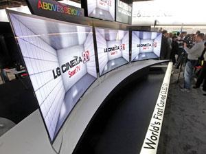
The Korean electronics giant has shipped over 300 million products featuring OLED displays, generating an estimated $7 billion (£4.5 billion) in global revenue in 2012. That success evolved over more than 30 years, with careful molecule selection and design giving OLEDs market-leading display quality. But with companies moving from pocket-sized displays to 55-inch-plus TVs, manufacturing problems remain to be solved.
LCDs typically shine a single white ‘backlight’ at viewers. Its light passes through a liquid crystal layer and the thin-film transistor (TFT) that controls the image signals, polarisers, diffusers and colour filters. By contrast, manufacturers can deposit separate 100nm-thick OLEDs directly onto a TFT. Each one lights up independently, without other optical components. That brings more vivid colours and truer black, faster response times that avoid blurring and suit 3D images better, and lower power consumption. ‘They knock your eyeballs out of your head,’ Forrest says.
OLEDs emit light through a process called electroluminescence: the recombination of an excited electron with a ‘hole’ left by the electron’s absence. On meeting in a molecule, the excited electron and hole sit in the material’s previously lowest unoccupied molecular orbital (LUMO) and highest occupied molecular orbitals (HOMO), respectively. The electron and hole bind together, becoming an exciton. When the electron fills the hole, the size of the energy gap between the LUMO and HOMO determines the colour of the light it releases.
Seeing the light
While scientists saw organic molecules electroluminesce in the 1950s, perhaps the first faint sign that it could be usefully harnessed came in 1979. At Eastman Kodak’s laboratories in Rochester, New York in the US, Ching Tang was struggling to develop organic photovoltaic cells. A mixture of polymer, absorbing dye and hole-transport molecules segregated into two separate phases gave slightly better results, and so he pursued the idea.
Kodak had a huge library of chemicals and they let me in with a UV light
Steven Van Slyke
And when Tang, now at the University of Rochester, connected up a later, more efficient two-layer cell to study current flow through it, he saw a dim glow that sparked his curiosity. One layer was transporting holes, and the other electrons, to the interface between the materials. There they recombined efficiently, allowing Tang to make light from organic compounds at much lower voltages than ever before. ‘This is today called an organic heterojunction, and almost all organic electronic devices have one,’ Tang says.
Unsure how to use the technology, Kodak hired Steven Van Slyke to help Tang. They chose materials to increase light output, lower drive voltage and therefore power consumption, and produce a stable device. ‘Kodak had a huge library of chemicals made over 100 years,’ says Van Slyke, now chief technology officer at Kateeva in Menlo Park, California, US. ‘They allowed me in with a UV light. Some bottles were clear and some had powder around the neck, so you could see the compounds getting excited.’
O for organometallic
Roaming this luminescent library, one uniquely fluorescent compound was obvious to Van Slyke: tris-8-hydroxyquinolinatoaluminium, or Alq3. Tang and Van Slyke found an Alq3 layer both transported electrons and emitted light. Putting an electropositive, or low work function, 10:1 magnesium:silver electrode on one side injected electrons into Alq3 well. On the other side, they put an aromatic amine hole transport layer, and finally a high work function transparent indium tin oxide (ITO) electrode to inject holes.1 Together, these elements powered ‘a huge jump’ in the resulting green OLEDs’ lifetime. ‘Most devices then lasted just minutes,’ Van Slyke says. ‘I remember being amazed that with those three components, we could turn the device on overnight and sometimes in the morning it would be a little brighter.’
By 1989 the Kodak scientists2 had doubled the internal quantum efficiency (IQE) of electrons producing photons to 2.5%. To do this, they modified their original design by doping the Alq3 ‘host material’ with fluorescent coumarin or conjugated dicyanomethylene molecules. ‘Introducing a small amount of highly luminescent materials in a host matrix, we could change colour and improve device efficiency and lifetime,’ Tang explained. That sandwich of hole and electron transport layers with a host–dopant emissive layer filling is still used.
Also in 1989, unaware of Kodak’s OLEDs, Jeremy Burroughes was working at the University of Cambridge, UK, to find an insulator to put in a prototype conjugated polymer transistor. His colleague, Donal Bradley, suggested polyphenylene vinylene (PPV), which he had worked with in his PhD. But they were also interested in its optical properties, for use in telecommunications. And when Burroughes applied an electrical field to PPV to test these properties, he saw light emission.
‘We then had to invent a way to use that discovery,’ recalls Bradley, who is currently the Director of the Centre for Plastic Electronics at Imperial College London in the UK. But rather than write a paper, Burroughes, Bradley and Richard Friend, who headed Cambridge’s organic semiconductor programme, wanted to patent their discovery first. That was not common at the time. ‘When we told the university that’s what we wanted to do, the response was “Why?”’ Bradley remembers.
The Cambridge team persisted, filing patents before writing a conventional paper describing a green/yellow device much simpler than Kodak’s small molecule versions, simply PPV sandwiched between two electrodes.3 They spun their patents off into a company called Cambridge Display Technology (CDT), which now also includes polyethylenedioxythiophene (PEDOT) hole transport layers in its polymer OLED sandwiches.
Brightening dim hopes
As the 21st century approached, OLEDs remained inefficient in spite of their early hopes, partly because fluorescence has a fundamental quantum mechanical limit. Singlet excitons, made when holes and electrons with opposite spins meet, are allowed to fall to the singlet ground state and emit light. Triplet excitons, made by holes and electrons with the same spin, are not. Recombination produces singlet and triplet excitons in a 1:3 ratio, limiting IQE at 25%.
The US scientists Stephen Forrest, then at Princeton University in New Jersey, and Mark Thompson, at the University of Southern California in Los Angeles, thought they could dodge this rule. First they made an unusually bright red OLED using a platinum-based dopant.4 They realised that near the large metal nuclei, excitons experience spin–orbit effects. Triplet excitons’ motion and spin interact with each other, nudging them to fall to singlet ground states and emit light through phosphorescence.
There’s a direct lineage between Samsung’s molecules and the ones that we developed
Stephen Forrest
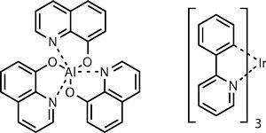
Then, in 1998, Thompson saw a green electrophosphorescent material’s optical properties presented at an American Chemical Society meeting. The team immediately knew the molecule, fac-tris(2-phenylpyridine) iridium (Ir(ppy)3), was an ideal phosphorescent dopant. And when Forrest’s student Marc Baldo, today a professor at the Massachusetts Institute of Technology, made an OLED with it, it smashed the IQE limit.5
‘[Iridium] is the key to everything,’ Forrest says ‘That one blew the lid off the field. It wasn’t long before we were demonstrating 100% IQE. At that point the OLED field took off as a practical solution for displays.’ Forrest and Thompson’s industrial partner Universal Display Corporation, also based in Princeton, has commercialised phosphorescent dopants, selling them for red and green subpixels in every Galaxy phone. ‘There’s a direct lineage between those molecules and the ones that we developed,’ Forrest says.
Beyond brightness, returning triplet excitons to ground state electrons also helps make OLEDs more stable. ‘Excitons are the biggest destructor of these materials,’ Forrest says. ‘They collide with an electron or another exciton, doubling their energy. If that energy couples with a bond on a molecule, it destroys that molecule. In a fluorescent material, the triplet can last for seconds, wandering around dying to do some damage.’
Making choices
Now that OLED displays are a practical reality, German company Novaled helps lower their power consumption further, bringing other benefits as it does so. Their transport layer materials, also omnipresent in Galaxy phones, contain small molecule organic redox dopants that smooth the journeys through devices taken by electrons and holes.
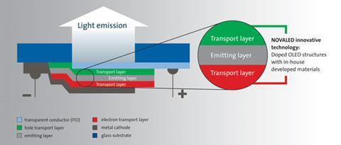
‘Electrode materials’ work functions are mismatched with the transport materials’ HOMO and LUMO levels,’ explains Sven Murano, vice president of product management for Novaled in Dresden. ‘We add strong electron donors on the electron side, and strong electron acceptors on the hole side, producing free charge carriers in the layer. That provides much greater freedom in choosing electrodes, and controlling charge carrier transport and energy level. Our technology allows new power consumption, colour quality and lifetime optimisation, and therefore better compromises.’
The chemical sandwich in the most common OLED displays is layered by evaporation in high vacuum tools onto electrode pads in TFTs previously deposited on glass substrates. That includes Novaled’s doped transport layers, formed by heating compounds until they sublime or evaporate, before they condense on a cooler target. However, that process can be difficult to manage.
‘There is a small temperature gap between evaporation and decomposition,’ Murano explains. ‘Manufacturers want to raise temperature to increase deposition rate and production speed, but at a certain level decomposition sets in. We are trying to widen that gap, which takes molecular design to find out where the molecule is weak, and propose new core structures.’
Samsung’s displays contain red, green and blue subpixels side by side. It makes them by vapour deposition, applying OLED materials in uniform films across a series of fine metal mask (FMM) stencils, one for each colour. ‘That wastes material, and the FMM can cause damage,’ Van Slyke says. But for making large TVs, the biggest problem is that FMM cannot get to larger mother glass substrates that can produce several 55-inch displays simultaneously.
Film stars
One alternative is to print the layers across larger glass sizes, and at Kateeva, Van Slyke is developing inkjet equipment to do just this. ‘Manufacturers like this because all the material ends up on the substrate, wasting far less, with the same appearance and same power consumption as shadow masking,’ he says. But it is difficult to control a printed film’s thickness and uniformity. ‘All the solvent has to evaporate, and there’s a lot, because you’re often at 1–3% concentration,’ Van Slyke says. ‘The resultant film must meet uniformity and thickness targets over the whole substrate. This is all possible with inkjet, but people are still working on it.’
One ink supplier is Sumitomo Chemical, based in Tokyo, Japan, which bought CDT in 2007. CDT’s polymer OLEDs are constructed from solution, enabling inkjet printing since 2004, including on flexible films. That requires layers coated later not to damage previous ones. ‘The chemistry is designing the polymer’s electronic structure,’ Donal Bradley comments. ‘But it’s also designing how peripheral polymer components control its processability. They control which solvents you can use and how soluble the polymer is in different solvents, to give layers you can deposit on top of each other.’
Though displays so far favour vacuum-deposited small molecule OLEDs over polymers, printing’s potential means that researchers are also developing it for small molecules. ‘The key question isn’t polymer versus small molecule, but solution versus vacuum,’ Bradley says. ‘At the Consumer Electronics Show in Las Vegas in January, Panasonic presented its 56-inch OLED TV, alongside Samsung and LG’s 55-inch models. The principal difference is that Panasonic’s is inkjet printed.’ Despite these announcements, he stresses that there’s more research to be done, for example on getting emission from triplets without using expensive iridium. ‘You might imagine that with a 55-inch TV commercial product there wouldn’t be much more science to do,’ Bradley says. ‘In fact there’s a lot more.’
OLED innovations also benefit other aspects of organic electronics, most notably photovoltaics. And even though that’s where Tang started out, he cautions success there could be harder than the display market. ‘Organic solar cells compete with silicon,’ Tang says. ‘OLED doesn’t. Other uses will have to find space, but OLEDs are finding real commercial applications. One thing you can be sure of: OLEDs will set the display quality standard for future televisions.’
Andy Extance is a science writer based in Exeter, UK


No comments yet