Fluorescent nanotube bundles could be used as chemical sensors or in optoelectronics
A team of scientists from India and Japan have been the first to make a bundle of nanotubes glow, paving the way for their use as chemical sensors and in optoelectronics.
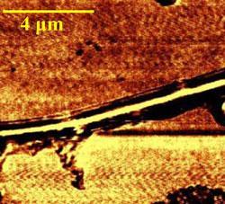
The researchers, led by Thalappil Pradeep of the Indian Institute of Technology, Madras, bound gold nanoparticles to single walled carbon nanotubes (SWNTs), which can be either metallic or semiconducting depending on how the carbon atoms that make them up are arranged. The nanoparticles increased the number of defects in the metallic nanotubes, making the entire bundle semiconducting and able to fluoresce.1
’The metal-semiconductor transition enables visible fluorescence by removing the nonradiative decay channels from excited states,’ Pradeep explained. ’The emission requires direct interaction of nanotubes with nanoparticles. It disappears when molecular spacers are introduced in between the nanoparticles and SWNTs.’
The fluorescence reported by Pradeep and his collaborators occurs in the visible region of the electromagnetic spectrum. Near infrared fluorescence has been observed from isolated SWNTs before but never from a bundle.2
Many of the currently envisaged applications in, for example, nanoelectronics, depend on being able to work with either semiconducting or metallic SWNTs but it has proved difficult to separate one form from another.
The new technique provides an easy, reliable way of converting metallic nanotubes into semiconducting ones, the scientists say. Vijayamohanan Pillai, a nanomaterials expert at the National Chemical Laboratory in Pune, said that the destruction of metallicity, allowing fluorescence, was an outstanding discovery, though he pointed out that the exact mechanism by which nanoparticles changed the SWNTs’ properties needed to be fully unravelled.
The bundles’ visible radiation allows them to be easily detected and mapped - of utmost importance when designing nanoelectronic circuits, said Pradeep. The fluorescence is also extremely sensitive to gases that interact with nanotubes. ’As fluorescence is such a sensitive analytical tool, combining the diverse properties of SWNTs with fluorescence will lead to a variety of applications,’ Pradeep said.
Chandrabhas Narayana, Pradeep’s collaborator at the Jawaharlal Nehru Centre of Advanced Scientific Research in Bangalore, said the next step would be to see if the bundles can be made to glow by passing a current through them.
’If the visible fluorescence can be excited by electrical means (electroluminescence) rather than light, it would immediately be applicable in semiconducting field to produce LEDs and lasers,’ he told Chemistry World. ’Currently, the yields by optical means, at least, are very encouraging.’
Jayaraman Killugudi
References
et al, Phys. Rev. Lett99et al, Science297, 593 (DOI: 10.1126/science.1072631)


No comments yet