A technique that separates semiconducting and metallic nanotubes could pave the way for progress in nanoelectronics
A new method for sorting carbon nanotubes could prove useful in creating nanomaterials for fast switching transistors, solar cells and touch screens, say scientists.
Nanotubes may have huge potential in electronics applications, but the manufacturing process produces mixtures of semiconducting and metallic nanotubes that are of little practical use.
Now researchers at Stanford University in the US and Samsung Advanced Institute of Technology in South Korea have developed a chemical technique for picking out semiconducting nanotubes from metallic nanotubes. ’For transistors it’s important to have only semiconducting tubes, but for conducting electrodes, like in solar cells, it’s important to have only metallic tubes,’ says Melburne LeMieux, who led the research.
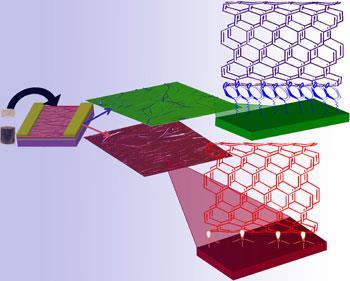
To sort the tubes, the researchers created nanometre-thick films on modified silicon wafers by spin coating, in which a nanotube solution is dripped onto the surface of a spinning wafer. Wafers with added amine groups attracted high densities of semiconducting nanotubes, whereas those bearing phenyl groups attracted the metallic nanotubes.
Although the team are still investigating the exact cause of the attraction, they think pi-electrons in the phenyl groups interact more strongly with the pi-electrons of the metallic tubes. They attribute the semiconducting tubes’ attraction to amines to electrostatic interactions.
The team have already made working transistors with purified semiconducting nanotubes. They also say they can fine tune the properties of their films, including the arrangement of nanotubes within them, by adjusting the spin coating conditions - from the speed of the spinning wafer to the density of the nanotube solution.
LeMieux believes the most immediate application for the method will be in enriching carbon networks with metallic tubes to make transparent electrodes for solar cells. ’This will probably be the first nanoelectronics application, rather than transistors,’ he says. The team are currently testing different functional groups to try to increase the density of conducting tubes in their films.
Peter Ashburn, who studies carbon nanotubes at the University of Southampton, says the study addresses one of the major challenges in nanoelectronics. But he believes other difficult problems remain. ’Solving the metallic-semiconducting split is an important step, but the main problem is that carbon nanotubes are just so variable,’ he says. ’It’s hype thinking that carbon nanotubes are going to go into industry for general electronics any time in the next 20 years.’
Hayley Birch
References
et alScience321, 101 (DOI: 10.1126/science.1156588)


No comments yet