Fine tuning the crystal structures of nanowires could boost the efficiency of LEDs and other electronic components
Dutch scientists have worked out how to fine tune the stripes of alternating crystal lattices that form in semi-conducting nanowires. Control of such structures could lead to important advances in electronics and optics, including more efficient LEDs, they say.
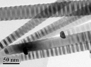
The researchers show they can change the spacing of stripes along nanowires made from indium phosphide, to create ’superlattice’ structures with regular segments of alternating crystal lattice. Scientists have theorised for more than a decade that such structures could prove useful in optics, but until now, they didn’t understand how to control the width of the segment in order to change the wire’s optical properties.
’The prediction is that if you could build superlattices with some of the materials that, for some reason, do not usually emit light at all, they could become emitters,’ says Lou-F? Feiner, one of the co-authors of the study based at Philips Research Laboratories in Eindhoven.
Feiner and colleagues found that two factors - nanowire diameter and the level of dopant - influence the spacing of the stripes. Crystals are doped with zinc to improve their conductivity; as zinc concentration increases, so does stripe width. The team also developed a model for layer-by-layer crystal growth, which they think will help them gain more control over the process.
Working by the same principles, Feiner hopes to make stripy nanowires from gallium phosphide, one of the best candidates for efficient green LEDs. Currently, green LEDs have to be made using a mixture of indium and gallium, but, explains Feiner, in such a non-pure system, the efficiency is limited. ’Ideally, we would like to have a material that is pure and still gives the right colour,’ he says.
Feiner says his team hasn’t yet considered the wider implications of their research in detail, but that the basic chemistry is the same for all applications of nanowires, meaning their work could be crucial to understanding how properties of wires could be controlled for electronics applications, such as transistors.
’These kinds of bottom-up approaches generate very perfect crystals and could be cheaper,’ says Georg Duesberg, a nanostructures expert at The University of Dublin. But, he adds, what is often forgotten amidst the excitement is that the standard silicon-based top down approach to making electronics is already very advanced and will be difficult to beat.
Hayley Birch
Enjoy this story? Spread the word using the ’tools’ menu on the left.
References
et alNature456DOI: 10.1038/nature07570)


No comments yet