Arrays of silicon wires can harvest light for solar cells much more efficiently than conventional silicon wafers, US researchers show
US researchers have designed a new silicon-based solar cell which uses 100 times less silicon than conventional photovoltaic devices. The system relies on the geometry of the silicon being reconfigured from a flat wafer to arrays of tiny silicon rods aligned vertically on the cell.
Currently silicon solar cells are fabricated on brittle wafers of silicon around 100-200 micrometres thick. While these can be relatively efficient in terms of conversion of light energy to electrical energy - up to 25 per cent - relatively large quantities of silicon material are needed, which is a significant part of the cost of the device.
Now Harry Atwater’s team at the California Institute of Technology has shown that far less silicon is needed if silicon wires rather than wafers are used to harvest the light. The researchers grew arrays of wires on a surface, around 0.5-2 micrometres in diameter and between 30 and 200 micrometres long, covering between 2 and 10 per cent of the surface.
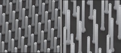
As light hits the arrays it bounces around between the rods until it is absorbed. Small nanoparticles of alumina are used as reflectors between the rods to guide the light more efficiently.
’We have shown the optical absorption efficiency and charge carrier collection efficiency of a silicon wire array cell is comparable to a conventional silicon cell, but a wire array cell uses up to 100 times less silicon due to enhanced light-trapping effects,’ says Atwater. Significantly, the wire arrays absorb infrared light more efficiently that conventional silicon surfaces, further improving the performance of the new device.
Using silicon wires, photovoltaic arrays can be manufactured on thin flexible films that can be rolled up like a plastic sheet but with optical and photovoltaic properties similar to a silicon-wafer-based device, Atwater suggests, adding, ’having demonstrated wire array growth, feasibility of device fabrication and optical absorption and carrier collection, what lies ahead is improved device design and engineering. The equipment toolset needed to do wire growth and photovoltaic manufacturing is all commercially available - an important consideration for scalability.’
Gianfranco Claudio, a photovoltaics expert at Loughborough University in the UK says that the silicon wire systems appear to overcome one of the big hurdles of conventional silicon. ’The biggest limitation for conventional silicon is that it is blind in the infrared region of the spectrum and so this light available from the sun is not converted to photocurrent. Silicon wires can capture the light from this region, potentially overcoming this inefficiency.’
Simon Hadlington
Interesting? Spread the word using the ’tools’ menu on the left.
References
M D Kelzenberg et al, Nature Materials, 2010, DOI: 10.1038/NMAT2635


No comments yet