
Whether atom-thick layers have the same neat lattice structure as the bulk material has been a long-standing question among materials scientists. New work shows that they do indeed.
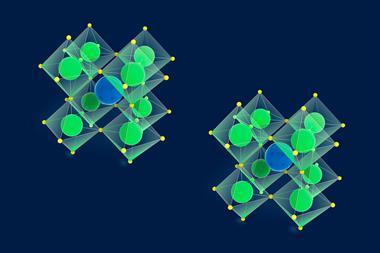
Perovskites are compounds comprised of two types of cations and one type of anion, like strontium titanate, SrTiO3. Unlike graphite, perovskites can’t be exfoliated to create 2D layers – the bonds between the individual layers are too strong. Now, material scientists from China and the US have for the first time created atom-thin strontium titanate and bismuth ferrite (BiFeO3) crystals.
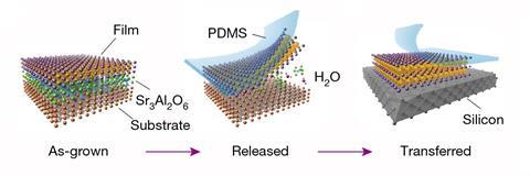
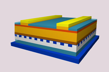
Instead of trying to shave down the bulk material, they grew the perovskites on a buffer material, strontium aluminate (Sr3Al2O6). The aluminate is water-soluble, so the perovskite films can be peeled off with tape once the material is submerged. The researchers then carefully transfer the square-millimetre-sized layers onto a silicon wafer or a holey carbon grid. Others had previously produced 2D perovskites, but had never been able to separate it from the support it was grown on.
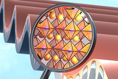
Electron microscopy revealed that the perovskites were nearly two-dimensional – two to four unit cells thick, only comprising a single atomic layer. Even at one unit cell thick, the materials maintain their ordered crystalline structure.
The 2D perovskites have some surprising properties not seen in the bulk material: bismuth ferrite has a different crystal structure and shows a large electric polarisation even in the absence of an electric field. Strontium titanate, a brittle ceramic, becomes flexible when grown as an ultrathin sheet.
‘We anticipate that 2D perovskite oxides could become as useful as graphene,’ the scientists behind the work write. They also hope to explore whether twisted perovskite layers behave similar to superconducting magic angle graphene.
References
D Ji et al, Nature, 2019, 570, 87 (DOI: 10.1038/s41586-019-1255-7)


No comments yet