Researchers have found an easier way of growing and printing nanotube circuits
Scientists in Israel have developed a simple way of making complex networks of carbon nanotubes and stamping them onto circuit boards, taking a further step towards building the next generation of smaller, faster microchips.
Nanotubes are strong, easy to make and excellent conductors of electricity but, to date, manipulating the tiny tubes has proven tricky. But now a team led by Yael Hanien at Tel-Aviv University in Israel has demonstrated a robust and cheap method of arranging carbon nanotubes on different surfaces.
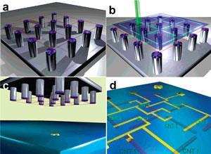
The researchers first grow nanotubes between silicon pillars, arranged to match the shape of the network they want. The nanotubes stick firmly to the top of the pillars, which are coated with silicon dioxide, and grow taught and straight between them.
Whether nanotubes behave more like a metal or a semiconductor depends on their chirality, so the team used Raman spectroscopy to check their properties with a laser. But in a neat twist, the team were also able to use the same laser to destroy any nanotubes they did not want and create a circuit free of defects. They then stamped the entire network onto a pre-made circuit board or onto a clean surface to which further circuitry could be added later.
The team are now trying to improve the stamping process to get a better imprint of the nanotube circuits. They also hope to find better ways of preventing the growth of stray nanotubes.
Dunwei Wang, a nanomaterials expert at Stanford University, California, told Chemistry World, ’This work provides a creative way to transfer selected nanotubes to a wide range of different substrates. It has the potential to be extended to other systems such as nanowires, but it still doesn’t address certain issues like density and uniformity. Nevertheless, this is a great preliminary step.’
’Depending on the application, we might see real-world uses in a few years, but for more complex tasks, it may be a decade or more,’ Wang added.
Lewis Brindley
References
et alNano Lett., (DOI: 10.1021/nl071058f)


No comments yet