Cheap flexible plastic is used in all electronic devices due to its flexibility and low weight. There are disadvantages to using plastics, which researchers hope to overcome by using paper substrates. Nanopaper is not only more flexible than plastic but is also easier to print on and more stable at higher temperatures.
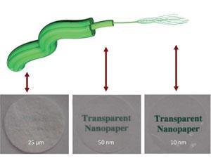
The key to high performing paper substrates is the diameter of the cellulose fibres – fibres with diameters much smaller than the incoming optical wavelengths achieve high optical transparency. This is desired in electronic displays for a clear picture, such as on a touch screen. A hazy substrate is desired in solar cells and anti-glare coatings, for example, where light needs to be absorbed. The large diameter of normal paper fibres unfortunately produces a lot of light scattering so it is always opaque, in addition to having a rough surface that is unsuitable for small electronic devices. By disintegrating the fibres down to the nanoscale, these properties can be controlled.
In this work, Zhichao Ruan from Zhejiang University and Liangbing Hu from the University of Maryland have looked at the effect of changing the fibre diameter and packing density in transparent nanopaper. ‘Specular transmittance measures light in the normal direction, whereas diffusive transmittance refers to the forward direction’ explains Hu. ‘As the fibre diameter decreases, the overall transmittance, including both specular and diffusive transmittance, increases. But the difference between the two, which is related to the haze of the nanopaper, starts to decrease.’
This tuning benefits a spectrum of applications in which clear or hazy substrates are needed. Daniel Lopez, an expert in nanofabrication and devices at Argonne National Laboratory, US, believes that the team have overcome ‘one of the critical technical barriers to the practical use of nanopaper, as the obtained level of over 90% optical transmittance opens up the possibility to use transparent nanopaper to display important information when it is needed, without the use of heads-up displays, micro-projectors or bulky electronics.’
The group are now continuing to adjust and improve the properties of the nanopaper, with an aim to apply it in devices such as thin film transistors.
References
H Zhu et al, Nanoscale, 2013, DOI: 10.1039/c3nr00520h


No comments yet