Masking metallic nanotubes reveals the true potential of their semiconducting neighbours
A new chemical process may help overcome one of the main obstacles to using carbon nanotubes in electronics, say US scientists. The technique suppresses the effects of metallic nanotubes, which can that can cause organic transistors to short circuit and could speed the development of semiconducting inks for low-cost, printable electronics.
Routes to manufacture single walled carbon nanotubes (SWNTs) typically generate a mixture of both metallic and semiconducting tubes, which differ in their arrangement of carbon atoms and so their electronic behaviour. The two forms have proven difficult to separate, and the metallic SWNTs disrupt the properties of their semiconducting neighbours, restricting their use in electronics.
One such potential application is in transistors, where two contacts - source and drain - are connected by a semiconducting material. This material must be able to switch rapidly between ’on’ and ’off’ states, while providing free passage for electrons between source and drain. But high levels of metallic nanotubes can reduce switching ability.
Now researchers at Cornell University, New York, and DuPont in Delaware, have shown it is possible to reduce the concentration of metallic tubes such that both high on/off ratios, and high electron mobility, are maintained.

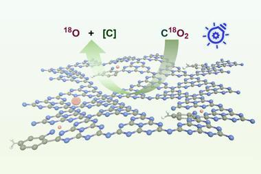
By carrying out cycloaddition reactions, the team anchored fluorinated olefins to the walls of nanotubes, before spin coating the resulting solution on to silicon wafers to make thin film transistors (TFTs). Lead researcher Graciela Blanchet speculates that the tails of the fluorinated molecules might get inside ’ropes’ formed between the two types of nanotubes and help to break them apart, although she has yet to figure out exactly how their method works. ’It’s not clear to us whether cycloaddition ’kills’ the metallic tubes - rendering them insulating - or converts them into semiconducting tubes,’ says lead researcher Graciela Blanchet.
Crucially, the reaction can be controlled so that only the metallic tubes are functionalised. ’The metallic tubes are more reactive than the semiconducting tubes so if you control the reaction very slowly, you can find a place in which the metallic nanotubes have been attacked and the semiconductors are intact,’ explains Blanchet. ’If you stop the reaction there then your array is only semiconductors.’
Although other groups have tried to improve electronic performance by functionalising nanotubes, the main difference is that Blanchet’s team use divalent functionalisation, bonding two molecules to each nanotube. This results in a dramatic improvement in mobility in comparison to monovalent functionalisation methods, says Blanchet, in addition to a high on/off ratio.
’The performance they got is definitely very impressive,’ says Zhenan Bao, a chemical engineer at Stanford University. ’High on/off ratio is important for most of the applications involving TFTs, so they did solve a very big problem,’ she says. She adds that although cycloaddition reactions of nanotubes have been shown previously, the electrical behaviour of the products has never been investigated.
But will the technique yield real world applications in the electronics industry? ’What they have shown is an important step, but of course, a lot more work will be needed to make it practically useful,’ says Bao.
Blanchet envisages semiconducting inks as the first application, although she admits a fully functional industrial device to print electronic circuits is a few years down the line. The long term goal, she says, is to use nanotubes to create cheap electronic materials that are as good as silicon - and the mobility of their current material, she adds, is already 100 fold higher.
Hayley Birch
Enjoy this story? Spread the word using the ’tools’ menu on the left.
References
et alScience323DOI: 10.1126/science.1166087)


No comments yet