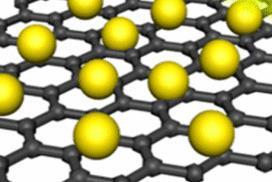
Graphene’s electronic structure is the subject of much study but it seems that this can be altered by the very scanning tunnelling microscopy (STM) tips used to probe it. When graphene is normally scanned by STM it’s supported by a substrate-like silica, but Jospeh Strosico and colleagues at the National Institute of Standards and Technology, US, and the University of Maryland, US, decided to lift their graphene off its support and instead suspend it in the air.
The idea behind the research was to remove interference from the support, but it also meant that the STM tip could deform the graphene lattice, creating a localised strain field. It turns out that that deformation is enough to separate the electronic states of the area, and with enough deformation create a quantum dot within the bulk lattice.
Being able to use the fast conduction of graphene and then, with deformation, create the band gaps needed for electronic components could lead to new graphene based devices. The work is published in Science.


No comments yet