Straightforward etching of sub-100nm structures onto diamond overcomes problems with defects
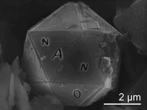
Scientists in Australia are the first to etch structures less than a hundred nanometres in size on the inclined surfaces of diamond by simply using a variable pressure scanning electron microscope (SEM). They believe their electron beam induced etching (EBIE) could make nanofabrication of diamond devices accessible to every nanotechnology laboratory in the world.
Diamond’s wide optical transparency window and high carrier mobility means that it’s a highly attractive material for optical and optoelectronic structures. But as one of the hardest and most chemically inert materials known, it presents enormous fabrication challenges. Current techniques involving ion bombardment or high power laser ablation that often cause surface damage and create artefacts from the redeposition of non-volatile, sputtered or ablated material.
‘We demonstrate a chemical approach that enables the fabrication of functional diamond structures using gas-mediated electron induced etching,’ explains team leader Igor Aharonovich at the University of Technology, Sydney. Key to their approach was the use of an electron beam in a water vapour environment. This was used to dissociate surface-adsorbed water molecules into radical fragments. The resulting volatile reaction products create voids on the surface when they leave the diamond substrate. By exploiting the high resolution, precise beam steering capabilities of an SEM, they were able to etch sub-100 nm lines on the inclined planes of a single crystal diamond.
Furthermore, spectral analysis revealed that the unique optical properties of diamond remained intact, indicating that no surface damage or redeposition had occurred, unlike standard techniques, which frequently implants gallium ions. ‘The exciting part is that the electron-beam etching avoids implantation of foreign ions,’ explained Christian Degen, whose research in nanometre scale spin detection at ETH Zurich in Switzerland, involves nanostructures made from single crystal diamond. However, given that many applications, such as micron-scale lenses and photonic crystals, take advantage of optically active defects in diamond, Degen would be curious to know what effect electron-beam etching may have.
Among such defects are nitrogen vacancy luminescence centres (NV) employed as spin qubits for next generation quantum devices. ‘EBIE may represent a unique advantage if the authors were able to demonstrate the fabrication of NV-containing diamond solid-immersion lenses without any risk of quenching the NV centre,’ agreed Ye Tao, a member of Degen’s lab.
For the moment, however, Aharonovich and his colleagues are continuing to investigate the universal appeal of EBIE as a technique for other wide band gap semiconductors. ‘EBIE can be applied to any system where a volatile reaction product can be formed by a dissociated precursor radical and target substrate material,’ he says.
References
A A Martin, M Toth and I Aharonovich, Sci. Reports, 2014, DOI: 10.1038/srep05022


No comments yet