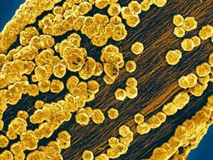
Today, steel wires with a diameter of 140µm slice up silicon ingots, but subsurface damage and variations in the thickness of 180µm wafers results in the loss of almost half of the material, according to Manuel Mee, project scientist at the Fraunhofer Institute for Mechanics of Materials in Freiburg, Germany. His solution is a CNT yarn encrusted with diamonds.
Growing diamonds on nanotubes is tricky, however, as they need to be deposited from a hydrocarbon gas onto a hot surface and the material ends up being a mixture of diamond and other carbon allotropes, such as graphite. The trick to get only diamond is to have a reactive gas atmosphere that selectively removes the non-diamond allotropes, but leaves any carbon with diamond bonding. ‘This is typically accomplished by having copious amounts of atomic hydrogen present. If you try to deposit diamond onto a non-diamond carbon surface [such as carbon nanotubes], you end up etching away the non-diamond carbon as you deposit the diamond,’ explains material scientist Nick Glumac at the University of Illinois, Urbana-Champaign, US. ‘You need a buffer layer to protect the non-diamond substrates.’ This is the secret of the new method, which was discovered serendipitously.
During early experiments, fused silica from the reaction chamber accidentally came into contact with the coating plasma. It settled on the substrate and protected it from the hydrogen. To the team’s surprise, diamonds grew on this layer. They then studied the silicon oxide layer in order to find a way of controlling the deposition and optimising the process.
Glumac describes the buffer layer solution as clever. ‘In terms of required developments,’ he adds, ‘I think you need to show the diamond has good adhesion and doesn’t degrade the mechanical properties of the underlying CNT wire.’ He adds that the proposed technique could probably be incorporated into existing wire-based cutting machines, though making continuous wires from nanotubes isn’t easy.
'At present, sawing silicon is a very well established and major industry where efficiency and reliability are critical to profitability,' says CSIRO's Stephen Hawkins. 'Replacing a significant part of this activity with CNT diamond saw wire will necessitate demonstration of substantially improved performance in these areas. Scaling and simplifying the production of CNT yarn and the diamond coating process are significant technical challenges before this demonstration can happen.'


No comments yet