Graphene is lauded for being an exceptional conductor and graphene nanoribbons could potentially succeed copper in nanoelectronics. GNRs are typically produced by exfoliating graphene. But this method produces relatively wide GNRs with disordered and defective edges, which causes high electrical resistance and poor charge carrying performance.
'While graphene sheets have been shown to have good transport properties in general, this is not the case for lithographically patterned graphene nanostructures,' says Walt de Heer, who led the research team at Georgia Institute of Technology, US. 'We have shown that graphene ribbons that are epitaxially grown on silicon carbide can, in fact, have transport properties that exceed theoretical predictions for perfect graphene.'
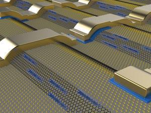
The team made their nanoribbons using a method that they first reported in 2010.2 This involved lithographically patterning electronics grade silicon carbide wafers to create a template with trenches that have sloped walls. The wafer is then heated, leading to the walls of the trench crystallising, followed by the growth of narrow graphene ribbons 40nm wide that, crucially, have smooth edges.
The GNRs resistance was tested by performing standard electrical measurements on them, similar to the way one would measure the resistance of a macroscopic wire. However, in this case, they needed the equivalent of an ohmmeter for nanoscopic objects. This required an electron microscope to position the ohmmeter leads.
'The biggest surprise is that the graphene ribbons behave like a single mode waveguide,’ explains de Heer. ‘For some reason, only a single quantum mechanical mode is involved and not at least two as expected theoretically.’
In exfoliated graphene, electrons typically scatter from imperfections and lattice vibrations; however, it appears that epitaxially grown graphene nanoribbons prevent such scattering of electrons. 'The transport appears to be protected. The mechanism that protects it is, however, not known,' says de Heer. What's more, the team observed transport at room temperature, which bodes well for applications. 'Theoretically, transport was supposed to deteriorate at room temperature due to lattice vibrations that become significant at room temperature,' he adds.
‘This is not easy to show, but de Heer and co-workers did it and it will serve as a landmark in the graphene field,' comments James Tour, who investigates graphene nanoribbons at Rice University, US. 'It is encouragingly revealing for the entire area of graphene-based electronics.'


No comments yet