A technique that grows gallium nitride crystals on glass could cut the cost of making LEDs
Korean researchers have grown crystalline gallium nitride (GaN) on the surface of amorphous glass. The idea could lead to new, scalable ways of making semiconductor devices that don’t need to be grown on silicon or sapphire wafers.
The technique uses a thin layer of titanium metal to provide a crystalline template for the GaN to grow on and a silicon dioxide layer patterned with tiny holes to control the shape and orientation of the growing crystals. This is essential to get LEDs that work well, explains Jun Hee Choi, who conducted the work as part of a collaboration between electronics giant Samsung and Seoul National University.
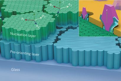
’When we deposit GaN directly on amorphous glass, we get a randomly oriented polycrystal morphology,’ says Choi. Because titanium’s crystal lattice has a similar size and shape to GaN’s, adding the titanium layer enables the team to control the orientation of GaN crystals on the surface. The titanium is followed by a thin ’nucleating’ layer of GaN grown at low temperature to provide an anchor for growing the larger crystals needed for LED devices.
A layer of silicon dioxide with an array of tiny holes is then deposited on top of the thin GaN layer. High temperature chemical vapour deposition is then used to grow the individual GaN crystals up through the holes. The crystals can then be processed by standard techniques to form LED arrays. ’The patterned silica layer and the titanium pre-orienting layer are both required to make single crystals,’ says Choi. ’GaN crystallinity strongly affects the efficiency of the final LEDs.’
But the complexity of the manufacturing process could cancel out a lot of the cost-savings of using glass substrates, says Colin Humphreys from the University of Cambridge, UK, who has developed ways to grow GaN LEDs on the large silicon wafers used by the microchip industry. ’It’s a lot of separate steps and if you have to take your specimen out of a reactor and put it into another piece of equipment, and then another, and another, that adds enormously to manufacturing costs.’
Choi admits that the performance of the LEDs is not quite as good as those grown on sapphire wafers, but points out that the work is still at proof of concept stage. He adds that the drivers for the project were not only cost and scalability, but also overcoming the scientific stereotype that single crystalline GaN can only be grown on lattice-matched crystalline substrates such as sapphire or silicon. ’Commercialisation will take at least 10 years,’ he says.
’It’s a long way from being a low-cost manufacturing route at the moment,’ Humphreys agrees, ’but they’ve made a very good start and the results are surprisingly good.’
Phillip Broadwith
References
J et alNat. Photon., 2011, DOI: 10.1038/nphoton.2011.253


No comments yet