The first materials to become less conductive when exposed to light have been created by researchers
Chemists in the US have created the first material to exhibit ’inverse photoconductance’, in which conductance decreases with exposure to visible light. The effect could be exploited to make new types of sensor that can be tuned for different spectral properties and printed directly onto plastic substrates.
Traditional photoconductors increase their conductance when exposed to light, and are typically made of a high-resistance semiconductor. When photons strike the semiconductor’s surface, they impart energy to electrons in the valance or conduction band. These energetic electrons then jump into the conduction band and, combined with the positive hole left behind, boost the semiconductor’s conductivity.
Now, Bartosz Grzybowski and others from Northwestern University in Evanston, Illinois, say they have made the first material that can reverse this effect. Unlike traditional photoconductors, the material is based on nanoparticles, and conductivity is governed by a phenomenon known as surface plasmon resonance. ’Because the wavelength of adsorbed light can be controlled by the nanoparticle size, we can flexibly engineer the spectral properties of these materials,’ explained Grzybowski. ’And because they are made of nanoparticles, they are flexible and can be printed onto plastic substrates.’
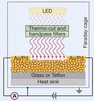
The Northwestern group makes the materials by mixing gold and silver nanoparticles with different alkane ’thiols’ - compounds similar to alcohols and phenols but with an oxygen atom replaced by a sulfur atom. The researchers apply these mixtures to substrates and evaporate off the excess solvent, leaving the nanoparticles spaced apart with thiol monolayers.
The origin of the inverse photoconductive effect, which they observe directly from electric current measurements, is an interplay between two mechanisms at the nanoparticle sites. When the researchers fabricate the materials using neutral thiols, incident visible light creates ’plasmons’ or plasma oscillations inside the nanoparticle cores, exciting electrons to the conduction band and providing normal photoconductance. However, when the researchers use positively or negatively charged thiols, the charges trap the excited electrons and conductance decreases.
Jeremy Baumberg, an expert in nanophotonics from the University of Cambridge, UK, finds the work interesting because charge transport in nanoparticle materials is often difficult to control, and because the tunability given by nanoparticle size might open up new possibilities for photoconductive sensors. ’However, the major problem is that the effects are produced by charge trapping around the molecular encapsulating layers, and the resulting devices are slow, [taking] several seconds to respond,’ he added. ’So it is not clear at the moment what impact they will have.’
Todd Krauss, a nanoscale materials researcher at the University of Rochester, US, calls inverse photoconductance a ’very interesting discovery’. ’From a practical viewpoint, the effect is tunable, both in magnitude and sign, by simply changing the [monolayers] on the nanoparticles making up the array,’ he said. ’Combine this tunable property with the inexpensive processing of solutions and there are some interesting applications that could come out of this work.’
Jon Cartwright
References
H et al, Nature, 2009, DOI: 10.1038/nature08131

No comments yet