Researchers have found a way to make smooth, patterned metal films that could be used in devices that manipulate electromagnetic waves called plasmons
US scientists have found a simple way to make smooth metal films with nano-scale patterns in a variety of shapes that could one day be used in plasmonic devices that manipulate electromagnetic waves.
The smooth surfaces allow these waves, combinations of light and oscillating electrons known as surface plasmons, to propagate further, and the patterning can be used to control and focus the plasmons, leading to enhanced sensitivity in applications such as spectroscopy.
David Norris and his group from the University of Minnesota, Minneapolis, combined the reasonably well known technique of template stripping (whereby a thin layer of metal is deposited on a very smooth surface made of mica and then peeled away to give a smooth metal counterpart) with various techniques for patterning surfaces. However, rather than making patterns on the metal surface after it is peeled off, they put the pattern onto a reusable smooth silicon wafer, so that when the metal is deposited and peeled off, the pattern is the same every time. The team produced a variety of patterns, including a set of ’bullseye’ concentric rings and arrays of bumps, holes and sharp-tipped pyramids.
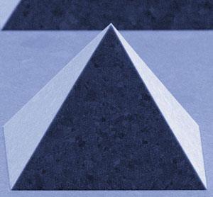
’Surface plasmons are like ripples on the surface of a pond,’ says Norris, ’we learn in school that a metal is a "sea of electrons," and if that sea sloshes back and forth and makes a wave, that’s called a plasmon. At the surface of a metal, you can get special waves that are a mixture of light and electronic oscillations, which are known as surface plasmons.’ Because they are part light, Norris explains that they can be excited by illuminating the metal surface, but because they have an electronic component, they can be focused into volumes much smaller than the wavelength of light. ’When you concentrate light in really small spaces, like the tip of a sharp pyramid, a lot of really interesting physics starts to happen,’ he adds.
But to be able to properly study plasmons and begin to contemplate real-world applications, there need to be simple ways of producing smooth surfaces with the right patterns on them. ’When you deposit thin layers of metals, they’re always a bit rough because they’re made up of tiny crystalline grains of metal’ Norris explains. ’Because surface plasmons are confined to just a few nanometres either side of the interface, any roughness can scatter them.’ He adds that most techniques for patterning the metal surfaces, such as lithography or etching with a focused ion beam (FIB), usually make the roughness worse and often involve destroying the patterning mould, so reproducibility can be a problem.
The group therefore exploited the property of noble metals such as gold, silver and copper to ’wet’ surfaces made from silicon - the metal particles spread out on the silicon surface, so if the silicon is smooth, the metal surface is the same. Usefully, these metals also don’t stick very hard to the silicon, so can be peeled off relatively easily to reveal the smooth surface. ’So you can take all the processes people have developed over the years to pattern silicon for microelectronics to put the pattern you want on the silicon, deposit the metal on top and then peel it off to reveal the smooth pattern’ says Norris.
Joachim Krenn, an expert in surface plasmonics from Karl Franzens University in Graz, Austria, is impressed by the range of patterns the group could create on the metal surfaces: ’I’ve never seen such nice examples of all these different geometries simply stripped off a template - especially the holes and pyramids.’ However, Krenn points out that while the surfaces are much smoother than many previous efforts, there is still some surface roughness in the order of 1-2 nanometres. ’When people talk about ultra-smooth surfaces, they normally mean atomically flat and this is a long way from that, but the range of geometries they can make is a real advantage.’
Norris agrees that their surfaces are still a little rough, but stresses that they’re just getting started with the technique. ’The biggest advantage of this technique is its reproducibility,’ he says, ’once you peel off the film, the silicon master is ready to go again and you can make several films that are nominally all the same, rather than having to start again from scratch the next time.’ He hopes that this will begin to enable people develop devices with consistent performance, but says that they still need to do a lot more characterisation work to find out exactly how robust the technique is.
Phillip Broadwith
Interesting? Spread the word using the ’tools’ menu on the left.
References
P Nagpal et al, Science, 2009, DOI: 10.1126/science.1174655


No comments yet