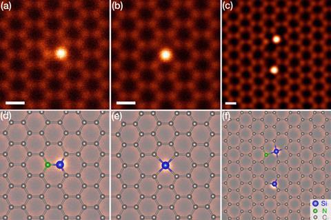
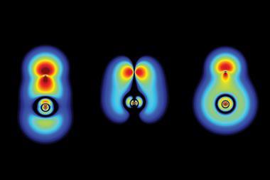
Stephen Pennycook and colleagues at Oak Ridge National Laboratory, Oak Ridge and at Vanderbilt University, Nashville, Tennessee, explain how investigating local structure and bonding characteristics at the atomic scale has become an important endeavour in materials science. Insights into the way in which impurities and dopants affect structure and bonding are critical to developing technological applications for a wide range of semiconductors and other substances, including graphene. They point out that various techniques have been tried and coupled to density functional theory (DFT) to underpin observations with theoretical foundations. Unfortunately, the electron microscopy techniques used so far have not allowed researchers to probe the bonding configurations of individual atomic impurities.
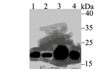
To overcome this problem, the Tennessee team has recruited atomically resolved electron energy-loss spectroscopy and annular dark-?eld (ADF) imaging carried out on a scanning transmission electron microscope. They demonstrated how well their approach worked by investigating one of the most common impurities in graphene formed by high-temperature chemical vapour deposition, silicon. Silicon impurities arise because the element is ubiquitous in the quartz components of the equipment used in CVD. The presence of silicon can affect graphene's properties and, given that the next likely step with microelectronics devices based on graphene will be their integration into silicon circuitry, an understanding of this element's behaviour in the two-dimensional carbon matrix is essential.
The team explains how ADF allows atom-by-atom chemical analysis, but the data reveals a planar image regardless of whether or not the silicon atoms are three or four coordinated. The spectroscopy also offers insights into the nature of the impurities corroborated by DFT calculations. The team suggests that the approach is ideally suited to two-dimensional materials like graphene, but might also be extended to the study of individual molecules in other two-dimensional materials.
Ute Kaiser of the University of Ulm, Germany, is enthusiastic about the potential of the research: ‘It is a very nice work and a further step in the direction of seeing bonds, not just atoms, in materials by using aberration-corrected technology.’


No comments yet