Thermoelectrics convert heat to electricity and can, therefore, ‘harvest’ waste heat from the environment. When one end of a thermoelectric material is heated, electrons flow to the cooler side, creating a voltage across the material that can be tapped for electricity.
The materials are rated according to the FoM, which depends on several properties. One is an ability to create a high voltage; another is a high electrical conductivity to allow a large electric current. But in the field of thermoelectrics scientists have focused on improving a third key property – a low thermal conductivity, which maintains the temperature gradient.
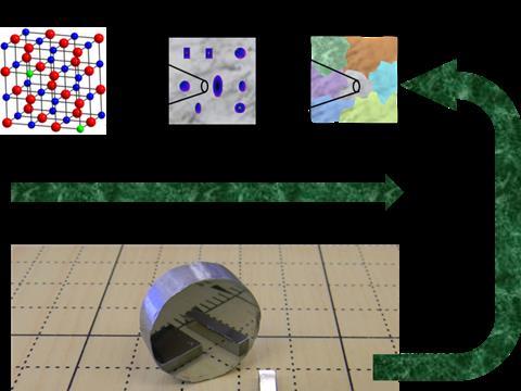
Heat passes through a material in the form of waves, or phonons, which have different wavelengths. To prevent the flow of heat, and thereby reduce the thermal conductivity, scientists must find ways to scatter these phonons. In the early days of thermoelectrics, scientists found that they could scatter the smallest-wavelength phonons by switching atoms in the materials’ lattices; this produced a maximum FoM of about one. Then in the early 2000s the maximum FoM shot up to roughly 1.8, with nanoscale crystals that could scatter the mid-wavelength phonons.
Mercouri Kanatzidis at Northwestern University in Evanston, Illinois, believes an FoM of two has long been considered a ‘psychological milestone’. ‘At two, the case for applications becomes much stronger,’ he says.
Kanatzidis and his colleagues have now succeeded in creating a material with an FoM greater than two by tailoring not just the atomic scale and the nanoscale, but the mesoscale too. They use sodium-doped lead telluride (PbTe) and strontium telluride – a mixture that, when frozen, spontaneously develops both atomic and nanoscale phonon-scattering structures. The researchers then grind the material into a powder that has larger grain sizes – large enough to scatter the largest-wavelength phonons. This hierarchical or ‘panoscopic’ approach produces an FoM of about 2.2.
‘Only a few years ago most of us believed sodium-doped PbTe could only achieve [an FoM of] 0.6,’ says materials scientist Jeff Snyder at the California Institute of Technology in Pasadena, US. ‘Now, for a number of reasons contributing together, we have [an FoM] of two.’ Snyder adds that an FoM above two ‘is not a rigid threshold for sudden adoption into applications’, but believes it is a ‘nice milestone’.
Materials scientist Eric Toberer at the Colorado School of Mines in Golden, US, points out that the new high efficiencies of thermoelectrics could make them competitive with solar cells. ‘One advantage is that solar thermoelectric generators do not require expensive thin-film growth,’ he says. ‘Rather, the desired nanostructures form spontaneously.’


No comments yet