Flat boron allotropes could find a future use in nanoelectronics
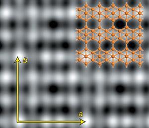
Recently, researchers synthesised the first flat form of boron – which could have interesting electrical properties. Now, a group at the Chinese Academy of Sciences has grown sheets of 2D boron that have a different structure.1
The team synthesised the flat sheets on a silver substrate using chemical vapour deposition with a pure boron source. Using scanning tunnelling microscopy observations and calculations, they showed the arrangement of boron atoms in the 2D sheets differed depending on the temperature of the substrate during the deposition process. At 570K, the boron atoms in the 2D sheet are arranged as rows of hexagons connected by boron ‘dumbbells’. When heated to 650K, a second form, comprising rows of boron ‘zig-zags’ is also observed.
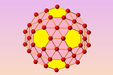
By contrast, the 2D boron made in November 2015 by Guoan Tai and colleagues was also grown by chemical vapour deposition, but in that case the team combined boron and B2O3 to make B2O2 vapour and reduced it with hydrogen while passing it over copper foil.2 Their 2D boron consisted of B12 icosahedra held together by B2 dumbbells.
Several other forms of 2D boron have been predicted using theoretical calculations. Researchers are hopeful that such materials could one day be useful for making nano-sized electronic devices.
References
1 B Feng et al, Nat. Chem., 2016, DOI: 10.1038/nchem.2491
2 G Tai et al, Angew. Chem., Int. Ed., 2015, 54, 15473 (DOI: 10.1002/anie.201509285)


No comments yet