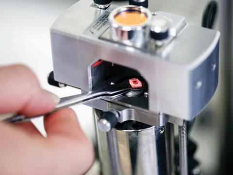
Their creators are the miniaturists of the modern era, though perhaps not as widely lauded. Since the 1980s, tiny stents have been inserted into arteries to prevent their collapse. But stents depend on even tinier, thinner drug coatings only 10µm thick for their effectiveness and without today’s high-powered microscopes, the drug-releasing coatings preventing artery closure might not be possible. Atomic force microscopy (AFM), which has developed over the same period as stents, allows the scrutiny of these minute activities in the lab.
‘How the drug is released can be difficult to analyse,’ explains Clive Roberts, chair of pharmaceutical nanotechnology at the University of Nottingham in the UK. ‘AFM allows us to analyse, for instance, how a certain coating releases a drug compared to another coating. You might think you know a lot about the sample but often there are things you are unaware of. It’s unsafe to assume a specimen is what you think it is in healthcare – you have to demonstrate it to the regulator.’
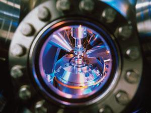
AFM is among the most recent major breakthroughs in microscopy and was commercially introduced in 1989. Perhaps still a specialist tool in life science applications, its use in the pharmaceutical industry is likely to increase. AFM instruments, part of a broader range known as scanning probe microscopy (SPM), work using a mechanical beam known as a cantilever. This has a probe at its end used to scan the sample surface. AFM measures a range of different forces between the probe tip and the surface. As the tip comes close to the surface, forces between the two make the cantilever bend and that motion is detected by a laser.
Atomic force microscopy
The advantage of AFM lies in its ability to scan at very high resolutions – fractions of a nanometre. AFM and SPM compete with or complement several other types of microscopes, which include optical microscopes in the life sciences. They may also be an alternative to scanning electron microscopy (SEM) in semiconductor production, polymer science and other material applications. SEM uses a focused electron beam to illuminate a specimen and produce a magnified image. All have progressed significantly.
‘SPM has developed dramatically since the late 1980s,’ explains Drew Murray, sales manager for instrument manufacturer Bruker. ‘Now it’s not just about looking at one material, but a range, and you can operate in different environments such as fluid, gas and controlled humidity.’ And that’s not all. ‘Previously the device measured just the topography of a sample,’ Murray continues. ‘Now it measures a whole range of different properties – mechanical, electrical, thermal and so on.’
Bruker is a leading producer alongside Agilent, Asylum, JPK Instruments and NT-MDT. Bruker managers are proud that scientists at the company improved the original SPM technique. Probes originally had to be physically in contact with the surface, and could therefore damage softer materials. They now commonly use a technique called tapping, invented at Bruker, which optimises characterisation of soft materials and in fluid environments. This has opened the door to greater use in the life sciences.
But there are drawbacks. AFM, for example, is considered a very specialist technique. ‘One of the biggest challenges for AFM is to make the platform more accessible to non-experts,’ comments Laurent Bozec, senior lecturer in biophysics and tissue engineering at the Eastman Dental Institute at University College London in the UK. For instance, a range of variables such as noise level and resolution have to be controlled by the operator. This means manually pressing a set of different buttons on the machine to get the desired image of the sample. Bozec, however, wants it to be usable by non-specialists such as clinicians in hospitals.
With AFM, you have to scan the probe over the whole image, which means it has always been slow
But Murray thinks Bruker has begun to solve this problem. ‘We’re making systems significantly easier to use. Previously you had to manually adjust feedback loops,’ he says. ‘Bruker has recently developed an algorithm called ScanAsyst that automatically optimises feedback parameters. We’re very optimistic this will extend the uptake to different industries not just in research but also in clinical work, quality control and even production.’
The Bruker MultiMode Dimension, FastScan and Bioscope Catalyst are all AFM instruments equipped with this patented feedback optimisation. Murray says industrial companies are using these capabilities to have instruments run automatically, unattended overnight.
There are other problems. Perhaps the biggest complaint is speed. ‘With AFM, you have to scan the probe over the whole image, which means it has always been slow. It takes five to 10 minutes per image; that’s difficult to get used to if you normally work with optical or electron microscopy,’ says Roberts, whose Nottingham department buys from Bruker, Asylum and JPK. Bozec, who buys and helps develop SPM tools, says AFM produces 12 images a day compared to 12 images an hour with SEM.
Murray suggests this is also changing. ‘Our products are developing a high-speed ability to take information several frames a second, compared to three to five minutes for other products. You can look at the dynamics of what is going on in that time frame – such as antimicrobial agents attacking bacteria,’ he says. The company claims its Dimension FastScan AFM achieves this goal, working hundreds of times faster than previous models. Scanning rates are up to several frames per second in air or fluid, while users also benefit from automated laser and detector alignment and comprehensive work flow.
Scanning electron microscopy
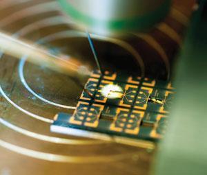
Electron microscopes are not considered to suffer from this disadvantage, however. This is because the whole sample can be snapped in one shot rather than scanned line by line. Major electron microscope manufacturers include JEOL, Hitachi and Carl Zeiss. Electron microscopes provide very fine images of specimens and with a wider field of view.
‘SEM in general simply has a much higher resolution [higher than 1nm] than light microscopes, allowing users to do a much more detailed analysis of their sample,’ explains Markus Wiederspahn, public relations manager at German instrument maker Carl Zeiss. ‘Besides visualising the surface of a sample, there are lots of detection modes, which also enable chemical analysis, for example.’
But they can be difficult for other reasons. ‘When you use SEM you are working in a vacuum. The sample needs a lot of preparation and has to be dead,’ he points out. This means SEM is more common in materials applications than the life sciences. It is often more expensive than AFM or light microscopes, but it may provide a facility lacking in the other types. This is exemplified by the Dual Beam system supplied by FEI, a company making electron and light microscopes, which looks within the sample.
‘The Dual Beam can cut into the specimen at specific angles and look below the surface. It can for instance measure layer depth, the inside of the specimen and run an analytical programme of each layer, such as the chemical composition,’ says Rod Shipley, FEI vice-president of sales and service. By contrast, much light microscopy and AFM provide an analysis of the surface only. Zeiss and FEI operate in some similar fields, though Zeiss is the bigger player. They provide different unique selling points.
‘The main advantage, which is unique to Zeiss, is that we offer three kinds of microscopy – light, electron and x-ray microscopy. We offer an interface from light microscopy to electronic using the ‘shuttle and find’ [correlative microscopy] facility which enables people to investigate samples with a light microscope, store the information and shuttle it to an electron microscope in a few mouse clicks,’ says Wiederspahn. He concedes that other companies also provide this, but says that Zeiss is unique in offering the platform all in one. ‘If you have two vendors, one offering each, they have to collaborate to develop the platform,’ he says.
Wiederspahn argues that the correlative facility, which has only been available since 2009, will change the nature of microscopy in many areas. ‘Having this possibility enables customers to do much more than they used to and will enable us to offer new services and approaches which could open up new application areas,’ he says. As an example, he suggests it could become particularly useful for pharmaceutical companies in drug development and in monitoring their own production processes.
Zeiss’ large size enables it to develop the technology and make acquisitions that may be beyond the capacity of smaller companies. This means products can combine different advantages. In one product, the Zeiss Crossbeam, SEM is combined with a gallium-focused ion beam column that enables it to cut through a sample. This makes it suitable, for instance, for gunshot residue analysis: ‘one of the hottest topics in forensics’, according to Wiederspahn. It allows finer chemical analysis so that researchers can better distinguish between gunshot residue and environmental particles. Meanwhile, the x-ray microscopy developed by Zeiss allows sample analysis without destroying the sample – which is not the case for SEM. ‘If you look at ball bearings and want to investigate them, once you open them, you have destroyed them,’ points out Wiederspahn.
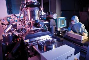
The company has also recently developed helium ion microscopy, which can be used to manipulate as well as inspect a sample. Its Orion Nanofab is a nanofabrication tool that integrates helium-, neon- and gallium-focused ion beams on a single platform. ‘This means you can manipulate the sample and change its properties; for example, you can drill holes into a membrane to produce sieves through which you could draw genes. This nanofabrication technology could drastically reduce the cost of genome analysis,’ says Wiederspahn. It could also be used to image shale and coal for oil and gas recovery and for semiconductor circuit editing and other tasks.
Other microscopes
Meanwhile, FEI is among the companies that produce transmission electron microscopes (TEMs). These massive machines, worth several million dollars, allow researchers in any branch of science and technology to study the internal structure of specimens down to the atomic level. Like AFM, TEM is sophisticated. ‘There might be 60 different buttons to tweak to get the best images. In the electronics industry environment that’s not going to work. If anything you need one black box and one button. But it’s becoming more user-friendly and has evolved for use by the electronics industry over the last four or five years,’ says FEI’s Shipley.
Light microscopes, the original microscopy technology, have also changed significantly in this very dynamic and innovative sector. They are produced by many different manufacturers, including Zeiss, Leica, Nikon and Olympus. ‘Optical microscopes are limited by the wavelength of the light, but they’ve changed a lot over recent decades. There’s been a huge jump in resolution and sensitivity down to single photon work,’ says Roberts. ‘You can now look at very small volumes of samples at high resolutions and there’s a lot of automation. Like AFM, it’s a very flexible working environment and is used on living cells in liquids.’
Roberts and Bozec are optimistic that the microscopes they use and buy will continue to progress. ‘We expect AFMs to become faster and record data of higher quality. There will be more automation. So long as you still have some control over it, that’s a good thing,’ says Roberts. Improved cantilevers from different component suppliers play a part, providing greater versatility. ‘They have varying sharpness and different tips – such as diamond or carbon nanotubes. This means you can look at a sample sideways, or they are very small so that you get an improved image,’ he explains. Meanwhile, correlative microscopy will bring in greater automation, speed and versatile functions, while real-time AFM use will allow the observation of dynamic interactions.
Bozec takes a similar view. ‘In future, more AFM settings will be automated and will be more widely available. There will be a simplified version of the instruments but the high end instrument will also be available for research scientists. If the technology can be presented more simply to clinicians, there is no reason why AFM should not move into every UK clinical lab as part of regular medical diagnostics.’
Elisabeth Jeffries is a science writer based in London, UK


No comments yet