Chinese scientists have developed a technique that can produce regular parallel arrays of graphene nanoribbons
Wrinkles are typically bad news for aging beauties and mechanical engineers alike, but researchers in China have controlled wrinkles in graphene to help make nanoribbons - a form of graphene that could help to produce faster electronics.
Graphene is an atom thick layer of carbon which electrons can move through easily. A sheet of graphene behaves like a metal, but in order to form logic gates it must act like a semiconductor. This can be accomplished by cutting the graphene into narrow strips. As the width shrinks below about 10nm, the electrons need more energy to get into the conduction band, where they move freely. Various groups have made graphene nanoribbons (GNRs), but they are tricky to position in parallel arrays.
Zhongfan Liu, of Peking University, China, and colleagues have developed a method to produce GNRs in this useful parallel arrangement. The team started by bending copper foil along parallel lines in its crystal lattice, making a ridged pattern. They vaporised carbon over the copper, to deposit a graphene layer on its surface. They then transferred the graphene to a flat silicon dioxide surface, leaving it pleated like a kilt. Air plasma was used remove the top layers of graphene until just the bottom layer of each pleat remained. The resulting GNRs were 7.4nm wide on average.
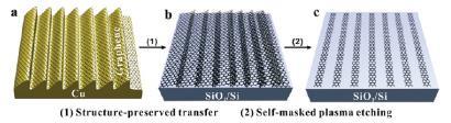
’The most attractive point of our wrinkle engineering approach is to directly produce large, parallel GNR arrays with a controllable density in a scalable and cost-effective way,’ says Liu. By changing the height and distance between the ridges in the copper, they can tune the widths and spacing of the resulting GNRs.
’This is certainly a clever technique,’ says James Tour of Rice University, US. He adds that, although the GNRs lack regular edges, which are desirable for better control over the array’s electronic properties, ’in the interim, it gets the community of researchers over some production hurdles’.
The team has already demonstrated a set of six GNRs working in a transistor, a device in which a semiconductor connects two electrodes, while a gating voltage determines whether the electrons can get into the conduction band or not. The GNRs always sent some current between the electrodes, but the gate had significant influence over the strength of that current, increasing it by up to a factor of 30 compared with when the gate was off. Liu says that by engineering narrower, more uniform wrinkles, his team should be able to produce transistors with even higher ratios.
Kate McAlpine
References
Z Pan et al, J. Am. Chem. Soc., 2011, DOI: 10.1021/ja207517u


No comments yet