Intricate nanowire shapes produced without templates or catalysts
Lead sulfide wires that sprout in intricate tree-like patterns show you don’t need templates or catalysts to control nanowire growth, say US-based chemists.
Song Jin, Matthew Bierman, and colleagues at the University of Wisconsin-Madison say their nanowires grow in ornate patterns of tall trunks and spiralling branches because of a defect intrinsic to the crystalline structure.
Growing nanowires in pretty patterns - including coils, flowers and belts - is not just a pastime for chemists with an artistic bent. Such branched building blocks have a large surface area, and can have unusual interactions with light. They’ve proven useful in photonics, solar cells, biosensors, catalysts and composites. But usually, Jin explains, pattern-growers need to add a second metal nanoparticle catalyst around which atoms will cluster to guide nanowires into particular structures.
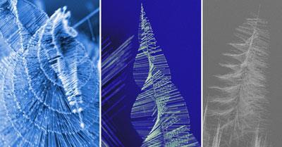
Not so for the lead sulfide pine trees. Jin’s team made the patterns by depositing lead chloride (PbCl2) and sulfur together onto a silicon wafer, from a 650? vapour shot through with argon and hydrogen gas for around half an hour.
As the crystals grow, a lead or sulfur atom slipping out of its regular position creates a ’screw’ dislocation that causes atoms to stack as if in a spiral staircase. At the edge of the crystal, the dislocation attracts atoms to stack preferentially on what becomes a quickly-growing trunk. The branches form more slowly by clustering around lead nanoparticles that are generated in situ as the crystal grows.
’The idea of using dislocations to drive growth in one dimension was known in the 1950s - and to some extent we have rediscovered it for nanowires,’ says Jin. ’We think these findings will motivate a lot of people to do this purposefully: to design dislocations and try to grow nanowires around them.’
But Jin is not yet sure how his team are encouraging the growth of dislocations. The hydrogen may encourage the emergence of the dislocation, he guesses, or dislocations may always be present in many nanowires, but the conditions aren’t always ripe for encouraging their growth.
Jin suggests that engineering defects in nanowires could also help chemists investigate the fundamental properties that dislocations bring to crystals. ’The mechanical properties of many materials are dominated by dislocations. Here we have the opportunity to isolate one dislocation in particular, rather than the millions found in large crystals,’ he adds.
’The research presents a significant advance for understanding the role played by dislocations in the growth of nanowires and their morphology evolution,’ comments Zhong Lin Wang at the Atlanta Institute of Technology, Georgia, who has studied nanowire growth as part of his research into creating nanowires that generate electricity when bent.
The interlaced lead sulfide wires may find application in high-performance solar cells, since they generate - and can quickly carry away - electrons when hit by photons of light. But as Jin admits, ’They’re beautiful and intriguing structures, but I don’t know at this point how useful they will be.’
Richard Van Noorden
Enjoy this story? Spread the word using the ’tools’ menu on the left.
References
Science, 2008, DOI: 10.1126/science.1157131

No comments yet