A new type of vacuum-based transistor can conduct electrons a hundred time faster than conventional electronics
Is your smartphone or your tablet PC still not quick enough for you? Then don’t worry, because scientists at the University of Pittsburgh, US, have come up with a new type of transistor that uses a vacuum to conduct electrons a hundred times faster than the conventional solid-state version. They claim that this new technology could open up a broad range of applications while being fully compatible with existing approaches to electronic circuit design.
The team has developed a low voltage field-effect transistor that, rather than being made of a solid state medium, has a vertical nanoscale vacuum channel etched into a metal-oxide semiconductor substrate. When fully optimised, the carrier transport time of the device – the key to high speed electronic systems – is just 100 femtoseconds, two orders of magnitude faster than state-of-the-art solid state transistors.
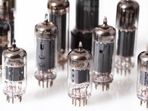
Transistors lie at the heart of almost all modern electronic devices, where they are used to amplify and switch electronic signals. Field-effect transistors use an electric field in a semiconductor material, usually silicon, to control the conductivity of a channel for the flow of charge-carrying electrons. However, the high electric fields needed to increase the carrier velocity in a solid-state material also increase electron scattering, which reduces the transistor’s effectiveness.
A vacuum is the ideal medium for carrying electrons at high speed as there is nothing to scatter the charge-carrying particles. However, vacuum electronic devices typically require a high operating voltage and are not usually compatible with solid-state transistor technology. The novel design of the new transistor, however, looks set to overcome these weaknesses and could enable a new class of low power, high speed devices.
The new technology will have a broad range of applications, says Hong Koo Kim, who led the research team. ‘Besides high speed and low power electronics, this finding will enable ultrafast, highly efficient energy conversion devices,’ he tells Chemistry World. ‘The process is compatible with conventional silicon electronics and can be easily implemented at low cost.’
Other researchers welcome the team’s discovery, but caution that further work is required. ‘This has great potential,’ says Jin-Woo Han, a researcher in nanotechnology at the Nasa Ames Research Center. ‘But two things need to be clarified: lifetime and integration. Any field emission device suffers from degradation, so the long-term stability needs to be guaranteed. The next big step is to build them into an integrated circuit.’
References
- S Srisonphan, Y S Jung and H K Kim, Nat. Nanotechnol., 2012, DOI: 10.1038/nnano.2012.107


No comments yet