Commercial solar panels are usually less than 20% efficient as they contain only one photovoltaic material. Photons with energies below the material's bandgap simply pass straight through, whereas part of the energy of photons with higher energies is lost as heat. Growing multiple thin layers on top of one another, so high energy photons are captured in a large bandgap layer on top, while lower energy photons that pass through are captured in a small bandgap layer underneath, can push efficiencies above 40%.
However, if different currents are generated in the different layers, charge builds up at the edges of layers, opposing the applied electric field and lowering the cell's efficiency. Therefore, the layers have to be carefully designed so that the currents match. ‘People have worked out how to manage this in two or three junctions,’ explains author John Rogers of the University of Illinois at Urbana-Champaign. ‘When you get to four, five or six, it becomes more and more daunting.’ Alternatively, one might keep the layers electrically isolated and harvest electrons from each layer separately, but no reliable industrial process exists for doing this.
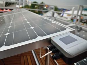
Rogers’ team, together with the solar cell companies Semprius and Solar Junction, started with a three-layer design that, until recently, held the world efficiency record at about 42%. They chopped up a germanium wafer into tiny pieces and mounted the individual cells in a printed circuit board arrangement. They covered the germanium wafers with a very thin layer of electrically insulating arsenic triselenide glass and used lithography techniques common to the semiconductor industry to print tiny versions of the three-layer cells on top. By imprinting small electrodes between the cells, they could collect electrons from the two cells separately.
However, the germanium cell underneath increased the overall efficiency by only about 1.8%. ‘This is a first demonstration out of the box,’ Rogers explains. ‘It's not a one-shot demo.’ He adds that independent cost projections suggest that ‘this technology is the lowest cost solution for climates that offer high levels of direct sunlight, such as solar cells deployed in arid environments [...] The cost of energy is projected to be lower than that of coal-fired power plants.’
Antonio Luque López of the Polytechnic University of Madrid agrees that value of the technique is in stacking electrically isolated cells. ‘In general, this is considered to be cumbersome and difficult to manufacture,’ he says. ‘They show that it could be easy to manufacture if you use microelectronic technologies.’


No comments yet