Troublesome clusters of dopant atoms 'seen' for the first time
Troublesome clusters of dopant atoms have been ’seen’ for the first time.
US researchers have drawn up the first 3D maps of the individual atoms in a semiconductor. These atomic plots are a crucial breakthrough in understanding how to make silicon transistors even smaller, said Keith Thompson of Imago Scientific Instruments, Madison, Wisconsin.
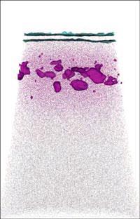
Microelectronic devices rely on atoms of ’dopant’ to provide the electrons that allow silicon semiconductors to perform their function. But dopant atoms tend to group together at defects in the silicon lattice, where they share electrons with each other instead of contributing them to the device.
’You put [the dopant atoms] in using a very well controlled process, but they can move around,’ said Thompson. This movement is only a few nanometers, but in the smallest devices the resultant clusters can have ’a huge impact on the overall properties, even to the point where it just doesn’t function,’ Thompson added.
Until now there was no direct way of telling how the dopant was distributed through the silicon. But the Imago team, in collaboration with researchers at IBM, used atom probe tomography (APT) to locate individual atoms of dopant, in this case arsenic. They were able to show that the arsenic atoms were forming spheroidal clusters around defects in the silicon.
Martin Castell of the department of materials at the University of Oxford, UK, congratulated the team on their achievement. ’Two critical things are starting to limit the development of semiconductors. They are dopant clustering, and our understanding of the statistics of dopant distribution. This paper addresses both of them,’ Castell told Chemistry World.
’Ten years ago it wouldn’t have mattered where the dopant was,’ said Castell, because the devices being made at that time were large enough that the average dopant content was more important. But with components getting ever smaller this information is becoming more and more important.
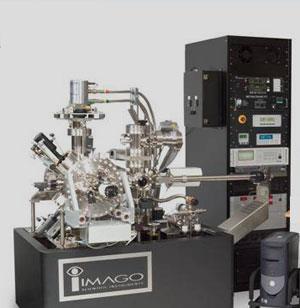
APT involves applying a high voltage to a cooled needle-shaped sample while hitting it with laser pulses. This provides enough heat energy to shoot the atoms towards a mass-sensitive detector, which identifies the atom. The atoms follow electrical field lines to the detector so their original location can also be deduced, eventually building up a 3D image of the sample’s atoms.
Thompson expects APT will be used widely to understand and improve the processing conditions used in semiconductor manufacture. ’In the next two or three years you will probably see that every major company will have an atom probe,’ he predicted. Castell said the technique ’is really going to take off, because it can answer so many questions.’
Tom Westgate
Enjoy this story? Spread the word using the ’tools’ menu on the left.
References
K Thompson et al, Science, 2007 (DOI: 10.1126/science.1145428)


No comments yet