DNA has been used to pattern silicon dioxide in an advance that could help manufacture computer chips
Researchers have used DNA nanostructures to create raised ridges and tiny trenches in silicon dioxide using an etching technique. The new approach cuts down on the number of steps needed and makes the process compatible with current silicon processing methods. This technique could one day be used to pattern computer chips.
DNA origami is an attractive technique for creating nanometre-scale structures, but the molecules are far more fragile than the materials with useful electrical and optical properties that they would pattern. Etching hard surfaces like silicon, without destroying the DNA in the process, is challenging. But now, Sumedh Surwade at the University of Pittsburgh and colleagues report a simple solution.
The key to the technique is the reaction between solid silicon dioxide and gas-phase hydrofluoric acid. These two molecules prefer to recombine as silicon tetrafluoride gas and water vapour, with water serving as a catalyst. ’The rate of this etching reaction critically depends on the amount of water on the surface,’ says author Haitao Liu. DNA and silicon dioxide both adsorb water, and their affinities depend on the humidity. In drier environments, silicon dioxide retains water better, but if the air is damp, more water clings to DNA.
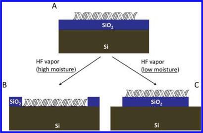
Liu’s team took advantage of this quirk to create raised and etched patterns in silicon dioxide using DNA. They first set folded triangles of DNA on the silicon dioxide. In the wetter environment, with a relative humidity of 50 per cent at 25?C, the hydrofluoric acid preferred to react near the DNA, digging channels underneath it. After washing off the DNA, the team used atomic force microscopy to reveal trenches about 17nm wide - roughly the width of the arms of the DNA triangle. Yet with a lower humidity of 30 per cent and at 30?C, the hydrofluoric acid etched the bare silicon dioxide faster. In this case, the triangular DNA protected the silicon, resulting in raised triangles.
’The method the authors have worked out is essentially kitchen chemistry,’ says Paul Rothemund of the California Institute of Technology in Pasadena, inventor of DNA origami.
Albert Hung, a nano-patterning researcher at the University of California, San Diego, calls the new technique ’elegant’, but he notes further challenges of DNA-based lithography remain, ’such as quality and consistency of the fabricated structures and reliable control of DNA deposition’.
Even so, Rothemund says: ’The method transfers the DNA pattern into the silicon dioxide, which is one of the most practically relevant surfaces since it is used in virtually all micro- and nano-electronic manufacture.’
Kate McAlpine
Interesting? Spread the word using the ’tools’ menu on the left.
References
S P Surwade, S Zhao and H Liu, J. Am. Chem. Soc.

No comments yet