Conventional small-scale fabrication techniques for nanoscale devices often involve toxic and corrosive volatile organic compounds (VOCs) that are used as solvents to etch or pattern surfaces. On such a small scale this use of VOCs is acceptable, but for industrial scale nanotechnology, there are significant environmental considerations. Even the development of quantum dot-polymer hybrids, DNA, and poly(ethylene glycol) (PEG) photoresists for nanolithography require noxious chemicals at various processing stages.
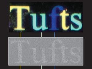
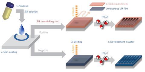
If VOCs and other toxic ingredients could be replaced by water, the environmental friendliness of nano-manufacture could be improved. But previous attempts to use water as a lithography solvent have led to low sensitivity, blurred lines and roughness, as well as scalability problems. Now, a team led by Fiorenzo Omenetto at Tufts University, US, has demonstrated that water can be used as the base for electron-beam lithography if silk, a natural material, is the target material with another acting as the mask for areas onto which the beam must not impinge. Self-assembled, crystalline silk, they explain, has several polymorphic forms, and its solubility in water can be fine-tuned using radiation.
The team used electron-beam lithography to fabricate nanoscale photonic lattices in silk supported on a silicon wafer or fused silica. In parallel experiments, they used neat silk and silk doped with various chemical and biochemical substances including quantum dots, green fluorescent protein and the enzyme horseradish peroxidase to show how the approach might allow biologically active nanoscale components to be produced this way.
‘I find this research extremely exciting,’ says Joanna Aizenberg, a materials chemist at Harvard University in the US. ‘Omenetto uses a very smart engineering approach to make a biological material do something it was not evolved to do – to provide a green solution to high-definition nanolithography that allows the formation of sub-50nm features using aqueous solvents. This is great stuff!’
References
S Kim et al, Nat. Nanotechnol., 2014, DOI: 10.1038/nnano.2014.47


No comments yet