New methods allowing researchers to sort metallic from semiconducting carbon nanotubes and to connect them to nanowires bring us a step closer to nanotube computers.
New methods allowing researchers to sort metallic from semiconducting carbon nanotubes and to connect them to nanowires bring us a step closer to nanotube computers. Michael Gross investigates.
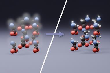
Electronic devices built from carbon nanotubes were the big nanotechnology sensation of 2001 and a deserving winner of Science magazine’s ’breakthrough of the year’ crown (Chem. Br., May 2002, p36). During that year, several research groups succeeded in building transistors from hand-picked semiconducting carbon nanotubes (which differ from their ’metallic’ siblings only in the geometrical arrangement of the graphite-type carbon hexagons with respect to the cylinder axis).
The main problem that stops researchers from scaling up the procedure and building complex circuitry or even computers out of nanotubes arises from the fact that the tubes are normally produced as random mixtures of metallic and semiconducting tubes with a range of different band gaps. While it is possible to measure the electronic properties of single tubes and then choose the right one for a given experimental set-up, any large scale application would depend on selective synthesis or efficient separation.
New reports from two different groups suggest different ways in which the selectivity problem can be overcome. The l ab of Nobel laureate Richard Smalley at Rice University in Houston, Texas, has shown that, once the clusters of nanotubes are disrupted by sonication of the suspension in the presence of the detergent SDS, the individual tubes are accessible to a reversible protonation reaction. Its progress can be conveniently observed by a change in the characteristic band gap fluorescence of the tubes. Interestingly, Smalley’s group showed that the reactivity of the nanotubes depends strongly on their electronic properties.
At neutral pH, metallic nanotubes react first. To protonate the semiconducting tubes, the researchers had to acidify the suspension. They observed that the reactivity decreased with increased band gap. This clear chemical distinction between the electronic variants suggests that suitable methods can be found to separate tubes using the protonation reaction. After separation, the protonation can be easily reversed by shifting the pH into the alkaline range.
Meanwhile, researchers at the Institute of Nanotechnology of the Forschungszentrum Karlsruhe, Germany, have already achieved a certain degree of separation using electrical fields. Like the US researchers, the team led by Ralph Krupke and Frank Hennrich started out by preparing a suspension of individual nanotubes using SDS and sonication. They placed a drop of this suspension on a chip carrier with microelectrodes to subject it to dielectrophoresis with voltages changing over a range of 10 V (peak to peak) at a frequency of 10 MHz.
After 10 minutes, they removed the droplet and investigated the chip using Raman spectroscopy and dark field microscopy. They concluded from their observations that metallic nanotubes, which only made up around a third of the original suspension, are selectively deposited on the chip, where they make up 75-85 per cent of the material.
Unfortunately, only a very small proportion (the authors estimate that 100pg out of 100 ng) of the nanotubes in the drop are deposited at all, so there is no significant enrichment of semiconducting tubes in the drop after the procedure. Given this proof of principle, however, it appears possible to develop improved methods of separation that will eventually provide electronically well defined samples of carbon nanotubes.
Once the nanotubes with the desired electronic properties can be obtained in high purity, there is another hurdle to overcome. If a semiconducting nanotube was simply plugged into an ordinary metallic wire, the so-called Schottky barrier - an energy barrier commonly found at the interfaces between semiconducting and conducting materials - would hinder the flow of electrons to and from the semiconductor. This phenomenon is well known from silicon electronics, where it is overcome by the use of wires made of doped silicon.
Hongjie Dai’s group at Stanford University now reports that circuits combining relatively wide (3nm diameter) single-walled carbon nanotubes with palladium contacts perform surprisingly well, suggesting there is virtually no Schottky barrier for this set-up. Electrons from the palladium contact - unlike other metals tested, including Ni and Ti - appear to enter the semiconducting tube just as easily as another conducting material. As yet, there is no theoretical explanation of why palladium should be so uniquely talented to link up to nanotubes, while other equally noble metals fail.
With these two major road blocks (almost) out of the way, nanotube electronics can move on rapidly. While the methods of sorting and connecting carbon nanotubes are being optimised further, and other researchers strive towards cheap and simple synthesis methods that can be scaled up to industrial production, somebody somewhere must already be drawing blueprints for the architecture of a nanotube computer.
Source: Chemistry in Britain
Acknowledgements
Michael Gross is the author of Travels to the Nanoworld and a science writer in residence at the school of crystallography, Birkbeck College, London. He can be contacted via the prose and passion web page.
References
1. M. S. Strano et al, J. Phys.Chem. B, 2003, 107, 6979.
2. R. Krupke et al, Science, 2003, 301, 344.
3. A. Javey et al, Nature, 2003, 424, 654.
4. A. Szabó et al, Phys. Chem. Comm., 2003, 6, 40.


No comments yet