Self-assembled semiconducting nanostructures with two distinct electronic domains form the first nanowire heterojunctions
Nanotubes sequentially grown from different components could lead to more efficient thin film solar cells, say researchers in Japan. The team is the first to form nanotubes which incorporate two electronically distinct semiconducting domains, an advance which could also see applications in devices ranging from solid-state lasers to transistors.
The nanomaterial’s properties centre on the fact that it incorporates a heterojunction - an interface between an electron-poor p-type semiconducting material and an electron-rich n-type semiconductor. Takanori Fukushima and Takuzo Aida at the RIKEN Advanced Science Institute and colleagues are the first to report such a nanowire junction.
These nanostructures could outperform bulk heterojunctions currently used in applications such as organic solar cells, Fukushima says. When a photon strikes an organic solar cell, an excited electron-hole pair is formed, the hole being siphoned into the p-type semiconductor and the electron to the n-type. The more efficiently that this process takes place, the lower the chance that the electron-hole pair will simply recombine, dissipating rather than harnessing the photon’s energy. Nanoscale self-assembly will allow the heterojunction interface to be deliberately designed to maximise electron-hole separation.
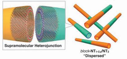
Creating the two-segment nanowire was a challenging process, Fukushima says. Their material is based on small graphene discs called hexa-peri-hexabenzocoronene (HBC), which self-assemble through pi-stacking interactions to form nanotubes. The team designed separate HBC derivatives to form the two ends of the nanotube. The first was fitted with bipyridine side-chains, which are known for their metal-binding ability. After assembling this end of the nanotube, the researchers added copper ions, which coat the outside of the tubes, stabilising them and preventing them from clumping together.
To this mixture of ’seed nanotubes’ was added the second HBC derivative, which had been fitted with four fluorine atoms. These electron-withdrawing groups help the second HBC molecules to electronically adhere to and grow from the end of the seed nanotube. The result is a segmented nanotube with the electronic properties needed to form a heterojunction.
Fluorescence quenching experiments show that excitation energy transfers readily from one nanotube segment to the other. In addition, light-generated electrons and holes were five times longer lived in the heterojunction material than in pure nanotubes, showing that effective charge separation takes place.
Devices based on nanoscale heterojunctions have great potential to outperform those based on bulk heterojunctions, says Zhen Li, who researches semiconducting nanowires at the University of Queensland in Australia. ’If they can fabricate devices such as transistors using these organic nanotubes it will be fantastic.’
Before the nanotubes can be developed into any kind of practical device, techniques will have to be found to make aligned arrays of the tubes, says Fukushima - an area that the researchers are now working on. ’If we can grow the nanotubes on a surface modified so that the nanotubes stand up, our control over alignment might be better,’ he adds.
James Mitchell Crow
References
W Zhang et al, Science, 2011, 334, 340 (DOI: 10.1126/science.1210369)


No comments yet