Photonic devices have the potential to transfer digital data up to 1000 times faster than conventional metal interconnects. However, diffraction and the wavelength of light limit the size of photonic devices, making them around 100 times larger than similar electronic components. Surface plasmon-based photonic devices, however, offer the possibility to confine light to sub-diffraction volumes using patterned surfaces. This allows for direct integration of high efficiency photonic devices with smaller electronic components.
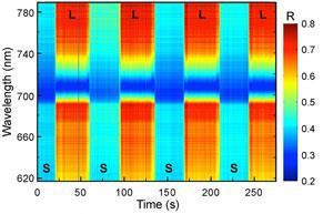
Now, Teri Odom, George Schatz and colleagues at Northwestern University in Evanston, have developed a method to produce nanoscale grating textures on liquid gallium surfaces. The grating structures exhibit reversible and switchable phase dependent plasmonic properties – that is, the liquid and solid phases of Ga show different plasmonic properties, with light coupling to form surface plasmon polaritons (SPPs) more efficiently in the liquid phase.
'Previous work on SPP propagation along a liquid metal surface was limited to excitation of SPPs in the far infrared, or required complicated set-ups,' says Odom. 'By monitoring the plasmonic properties at the Ga-dielectric interface during the phase changes, we observed a significantly larger switching contrast between the liquid and solid state than any other reports.'
The team made a polyurethane template of the desired grating structure, then moulded liquid Ga against the template. By filtering the Ga to eliminate surface oxide impurities, the team could pattern Ga in gratings with 400nm periodicity and sub-100nm features.
'While the optics of a plasmon is widely accepted and understood, the processes by which a plasmon can interact with the wider environment are not so well understood in a number of cases – most notably catalysis – and so any new technique to produce a plasmonic surface is of great interest,' comments Steve Dunn, who investigates nanomaterials at Queen Mary University of London, UK. 'This work makes a further contribution by aligning the modelling of the system with experimental evidence – notoriously difficult for a system of this type.'
'Until methods to directly manipulate plasmonic properties via fast switching rates, on/off contrast, and materials stability are realised, plasmonic circuitry will never be able to replace current metal interconnects,’ says Odom. ‘Using phase change as a switch presents a first solution to this problem.'
James Urquhart


No comments yet