New polymer semiconductor promises to boost the processing power of printed circuits
The prospect of powerful electronic circuits made from printable plastics has moved a step closer with the discovery of a cheap, stable organic polymer semiconductor that carries charge through the movement of electrons. The material complements the range of printable organic semiconductors that operate by conducting positive charges or ’holes’ - opening the possibility of far faster printed circuits based on transistors which combine the two materials.
A team led by Antonio Facchetti, of the Polyera Corporation in Illinois, US, has shown that a polymer based on naphthalene-bis(dicarboximide) can be readily processed by a range of printing technologies, including ink-jet and gravure printing, and combined with other components to create ’complementary’ circuit components that use both electron-transporting and hole-transporting polymer materials.[1] The potential of naphthalene-based polymers to act as electronic conductors was first reported in 2008 by Xugang Guo and Mark Watson of the University of Kentucky.[2]
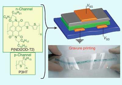
’For high performing transistors it is necessary to have both hole- and electron-transporting materials, called p- and n-channel transporters, working together in a complementary circuit,’ Facchetti says. ’At the moment only p-channel polymers are available; n-channel materials have proved problematic and challenging - they needed to be created under vacuum or nitrogen,’ he adds.
The new class of compound has two key features: it can accept low-energy electrons readily, and is highly ’regioregular’ - it forms a highly ordered polymer backbone with no distortions, enabling charge to be transported down the polymer chain extremely efficiently.
The reason it is able to accept electrons easily is that four C=O bonds surround the central core of each building block of the polymer. These pull electrons away from the centre, resulting in an electron-depleted region. Low-energy electrons can therefore drift with little impediment into the core of the molecule and be passed along the chain.
Future functions
Facchetti points out that plastic semiconductors are unlikely to replace silicon and other inorganic materials in devices such as PCs and mobile phones. Rather they will find applications in new areas, such as in organic display devices and sensors.
Martin Grell, an organic semiconductor specialist from the University of Sheffield in the UK, is impressed by the work. ’The material and its characteristics are very good, and it’s good to see multiple processing techniques and complementary devices demonstrated as well,’ he adds.
Simon Hadlington
Enjoy this story? Spread the word using the ’tools’ menu on the left.
References
23, 5333, DOI: 10.1021/01801918y
No comments yet