New method can produce bilayer graphene with potential applications in optics
A new, scalable way of producing a type of bilayer graphene with potential applications in electronics has been developed by researchers in the US and Asia.1 The technique could potentially allow for tuneable transistors and spectrometers.
The appeal of graphene for electronics lies in its extremely high electrical conductivity. However, it is difficult to reduce this and create an ‘off’ state. In 2009, researchers in California offered a potential solution, showing that an electric field perpendicular to the layers of bilayer graphene opens an energy gap between the valence and conduction bands, reducing the conductivity significantly.2 But this only works when the two graphene layers are in the correct relative orientation. Graphene is usually produced commercially by chemical vapour deposition (CVD), in which graphene crystals nucleate on a substrate when vapour passes over it. Graphene crystals grow with variable orientations, making the relative orientations of the upper and lower layers difficult to control.
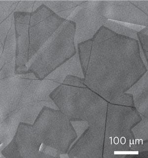
In the new work, researchers in the US, China and South Korea folded a copper substrate containing oxygen impurities into a ‘pocket’, allowing gas to enter only through a tiny gap at the edge, before placing the pocket into a CVD chamber. They introduced methane and found that, after six hours, the exterior surface was completely covered with graphene, with a high density of islands of single-crystal, correctly-oriented bilayer graphene. Subsequent experiments and modelling showed that monolayer graphene forms relatively quickly on the outside but, because of the restricted flow to the interior, it forms much more slowly inside the pocket. However, the oxygen impurities on the copper oxidise the methane, leaving carbon atoms on the copper foil. These carbon atoms gradually diffuse through and along the foil, forming a second layer of graphene underneath the first layer on the exterior of the pocket.
The pocket produced graphene had electrical properties that were comparable to those of graphene produced by mechanical exfoliation from bulk graphite. Team member James Hone of Columbia University in New York says that the band gap – about 125meV – is not, on its own, high enough for a transistor, although the tunability could be useful. He believes the initial applications will lie in optics: ‘Now we can take one pixel and change its sensitivity across the spectrum,’ he explains. ‘You can imagine making an infrared spectrometer by adjusting where the detector is sensitive.’
Andrea Ferrari of the University of Cambridge, UK, who was not involved in the research, agrees with Hone that potential applications are in optics. Regarding electronics, he says: ‘It is clearly a step towards having usable graphene technology, but it’s not the final step.’
References
1 Y Hao et al, Nat. Nanotechnol., 2016, DOI: 10.1038/nnano.2015.322
2 Y Zhang et al, Nature, 2009, 459, 820 (DOI: 10.1038/nature08105)


No comments yet