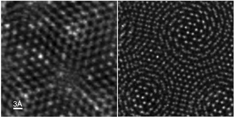
Single-atom defects visualised in a molybdenum disulfide monolayer in unprecedented detail using electron microscopy
US scientists have taken the highest resolution electron microscopy (EM) image of a 2D material to date.1 Using a special detector design and a technique called ptychography, the researchers were able to significantly increase the quality of EM images at low beam energies. The new method will enable 2D materials to be studied in exquisite detail for many applications.
Scanning transmission electron microscopes are widely used to characterise nanoscale structures, but their lenses have intrinsic imperfections known as aberrations, so special correctors are required to improve their resolution. Normally, the performance of a microscope depends on the aperture of the lens and the energy of the electron beam, so the image resolution has traditionally been improved by increasing these two parameters. Using aberration correctors, the resolution reached 0.47Å at a beam energy of 300 keV in 2009.2,3 This is enough for imaging most bulk materials, but 2D materials are sensitive and require lower beam energies (around 20–80keV), so for them, the spatial resolution has remained lower, at 0.98Å.
Now, a team working with David Muller at Cornell University, US, has resolved the distance between atoms in 2D molybdenum disulfide (MoS2) at a resolution of 0.39Å using a beam energy of only 80keV. ‘Muller et al. have developed new instrumentation that has produced the most accurate, high-resolution EM image ever recorded,’ says John Rodenburg at the University of Sheffield, UK. ‘The technique also requires fewer high-speed electrons to make the image —good, because these can damage the specimen.’
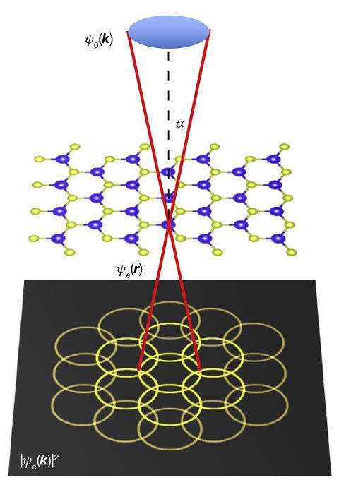
‘The key to the experiment is our new detector design,’ says Muller, referring to the electron microscope pixel array detector (EMPAD) developed at Cornell. The technique works by firing radiation through lots of different patches of the object and then measuring, using the detector, how the radiation has been deflected by the object. The radiation mixes up and interferes with – or ‘folds into – itself (ptycho is the Greek for ‘fold’) before reaching the detector. A computer then unravels all the mixed-up waves to make a perfect image.
In this system, the resolution is set by the largest recorded scattering angle and is no longer determined by the angular limits of the lens, says Muller, which leads to a 2.5X improvement in the resolution. The team used 2D materials to measure the limits of the method. ‘Essentially, we used a twisted bilayer of MoS2 as the world’s smallest ruler, giving us a test object where the projected distances between atoms could be made arbitrarily small,’ Muller explains.
Their results demonstrate that ptychography can provide very good images without good lenses, outperforming traditional techniques such as annular dark-field (ADF) imaging.
Although the theory of ptychography has been known for several years, Muller says that a detector with the speed and dynamic range required to achieve this resolution was missing. ‘Our EMPAD has the sensitivity to record the full scattering distribution needed, without saturating, and the speed to collect the data before the experiment drifts out of alignment.’
References
- Jiang et al, Nature, 2018, DOI: 10.1038/s41586-018-0298-5
- Erni et al, Phys. Rev. Lett., 2009, DOI: 10.1103/PhysRevLett.102.096101
- Sawada et al, J. Electron Microsc., 2009, DOI: 10.1093/jmicro/dfp030


No comments yet