
The rapid expansion of electronic and microelectronic technologies over the last century has transformed the way that we communicate and connect with the wider world
From sending an instant message to holding video conferences, technology has transformed how we communicate. The innovation that we see in modern wireless electronic devices and networks – such as computers, satellites and mobile phones – is not only connecting us but amplifying the voices of people around the world. These advances in wireless communication devices are underpinned by the semiconductor industry’s ability to continually modernise.
As you may remember from your high school lessons, the term semiconductor refers to a material that can partially conduct current. The conductivity of a semiconductor falls between that of an insulator – which has practically no conductivity – and a conductor, which has close to full conductivity. The specific properties of the semiconductor can be altered through the introduction of dopants into the structure of the crystal. The ability of a semiconductor to conduct current is dependent on temperature and dopants found on the semiconductor, which allows it to be a good medium for the control of electrical current. Because of this, semiconductors are now a fundamental element of integrated circuits in almost all electrical devices. Essentially, semiconductors are the backbone of modern communication.
Since the 1960s, Moore’s law – the principle that the speed and capability of computers can be expected to double every two years as the number of transistors a microchip can contain increases – has served as a guide for semiconductor production and encouraged the development of smaller and more intricate microchips. But as semiconductors continue to shrink in size, it has begun to falter against the laws of physics. So, new materials and fabrication techniques must be developed to ensure continued advances in these devices. Here at Umicore, we are committed to developing environmentally friendly practices that allow this innovation to progress.
The thin films that connect us
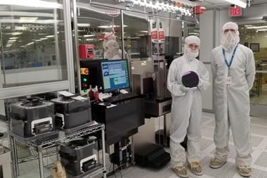
Semiconductor device manufacture begins with the deposition of extremely thin films of material onto wafers, which are often made of silicon. Within the industry, physical vapour deposition (PVD) processes are widely used to fabricate these thin films. However, for 3D structures, these techniques suffer from limitations because PVD is a ‘line-of-sight’ technique and is therefore not an ideal choice for coating non-visible surfaces, such as deep trenches. In these applications, chemical vapour deposition (CVD) is a more favoured technique. In comparison, CVD provides a milder process that not only forms these thin films but can also produce conformal 3D films with a greater ease. In this process, volatile precursors – such as organometallics or metal complexes – are passed over a heated substrate where the thermal decomposition of the precursor produces a thin film which is deposited onto a silicon wafer.
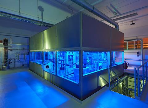
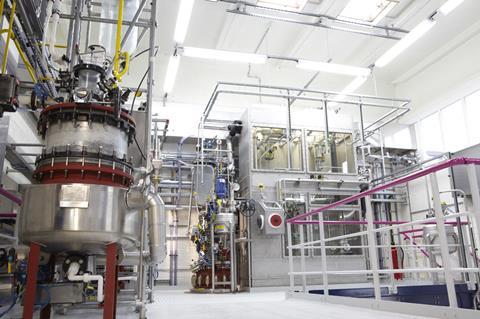
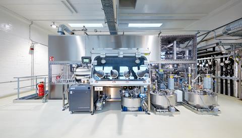
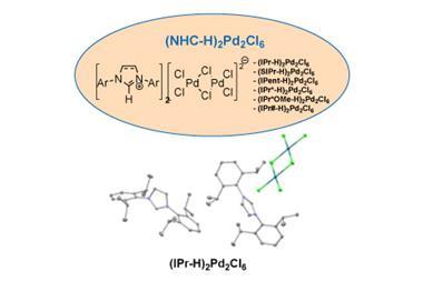
High-purity precursors are crucial to CVD. With increasingly small semiconductor devices, impurities in the parts per billion range can have a devastating effect on semiconductor performance. Precursor materials are volatile and consequently require specialised equipment and know-how for manufacture and transportation. Additionally, precise attention must be given to the manufacturing process due to the high purity requirements of these materials for semiconductor fabrication. At Umicore Precious Metals Chemistry, we leverage our experience in volatile organometallic and catalysis chemistry to ensure that we can provide highly pure precursors and offer better performance, all at a lower cost to the consumer.
27 Co-mmunication
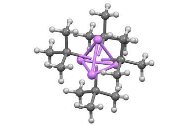
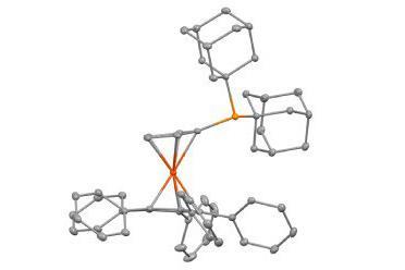
Cobalt-based precursors are an important organometallic precursor that we offer. Most modern computer chips contain copper as interconnects. However, as semiconductors reduce in size, manufacturers often increase the electric current to increase the power output. This can lead to electromigration of the copper into the silicon. To combat this, manufacturers can add cobalt layers to serve as a liner. Here, cobalt acts as a barrier layer to prevent electromigration of the copper into silicon. However, working with cobalt material is not simple. A common intermediate for cobalt precursors is cobalt carbonyl, but this compound is very difficult to handle due to its toxicity and hazardous potential. Additionally, the limited stability of the intermediate has led to the supply gap for this material.
Tackling the environmental impact of the electronic industry is incredibly important
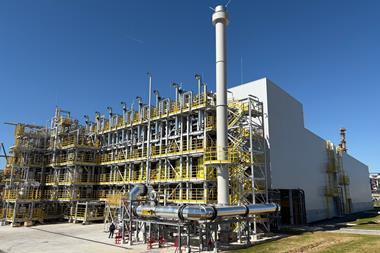
For over 100 years, Umicore has been a world leader in cobalt products. Across many business units, we produce a wide range of cobalt-based chemicals for varied applications. We decided early on to build an ethical and auditable supply chain. In 2004, we became the first company to introduce a specific approach to sustainable and ethical cobalt sourcing. This led to the foundation of Umicore’s current sustainable procurement framework for cobalt. This strategy provides safeguards that help to ensure a robust supply chain for cobalt products. It also guarantees that end users receive their required product in a consistent quality and quantity.
Tackling the environmental impact of the electronic industry is incredibly important. Due to the high number of electronic devices in the world, small improvements in sustainability can have wide-reaching impact. We sustainably manufacture electronic precursors on a large scale and recycle through a sophisticated nonferrous metals recycling group. Umicore also handles toxic and sensitive organometallics with expertise.
The future is calling
Many consider the invention of the transistor in 1947 as the starting point for the digital revolution. Since then, silicon semiconductors have played an indispensable role in the global communication networks that are essential in our lives today. However, as mobile and wireless communication becomes more data focused, there is a growing need to increase data traffic and implement higher speed networks. During 2019, various mobile network operators announced plans to roll out 5G technologies to selected cities around the world. This new generation of cellular technology will use a much wider range of frequencies than its predecessor, allowing a greater number of devices to simultaneously connect to data networks.
Compound semiconductors are important for the deployment of 5G technology. Alloys, such as gallium arsenide and gallium nitride, already complement silicon in applications like wireless communications where they enable high speed and efficiency. These compounds offer enhanced performance compared to traditional semiconductors comprised of silicon only. Of these materials, III V compound semiconductor have received great interest for potential application in wireless communication. These alloys combine a group III element with a group V element.
Our solvent-free method offers more ecological production by minimising hazardous side streams and increasing atom economy to nearly 100%
One advantage of compound semiconductors – seen in gallium arsenide – is a higher electron mobility than silicon. This feature allows them to be much more useful at higher frequencies than traditional silicon semiconductors. Another advantage – seen in gallium nitride – is insulating properties. This allows for the creation of power devices that can efficiently transform electricity to a higher or lower voltage output. Compared to silicon semiconductors, gallium nitride can be up to 10 times more efficient in power conversion.
Historically, compound semiconductors were not widespread in commercial applications due to the high cost and difficulty in manufacturing alloys. However, this has now changed due to metalorganic CVD (MOCVD), which is a modern process for the fabrication of compound semiconductors. In these methods, high-purity organometallic precursors are reacted with gaseous phosphine and arsine precursors. Umicore provides an innovative and sustainable organometallic precursor manufacturing process to enable MOCVD. Our solvent-free method offers more ecological production by minimising hazardous side streams and increasing atom economy to nearly 100%. As a result, our method allows us to offer our precursors at incredibly high purity levels.
Supported by the rapid innovation in semiconductor fabrication, the market for electronic communication devices continues to grow at an incredible pace. Developing materials and technologies such as cobalt alloys, compound semiconductors and MOCVD is helping to further this growth. These innovations must be underpinned by green and ethical practice. By creating sustainable solutions, we can help improve tomorrow’s world and communication.
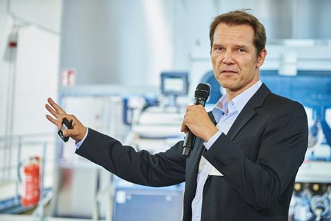
Oliver Briel is the director of global business electronics at Umicore Precious Metals Chemistry


No comments yet