
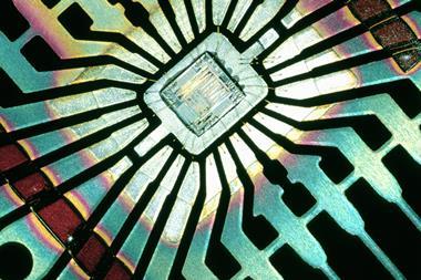
Carbon nanotube (CNT) transistors have been produced in commercial silicon chip facilities by US researchers, marking possibly the first time a post-silicon transistor intended for use in a computer processor has been made in this way.1 This is a milestone for CNT transistors as it shows that they are compatible with current manufacturing processes.
The transistor is the foundation of digital logic: a switch that either allows through or blocks current. In a computer processor, transistors connected in sequence execute the long chains of conditional operations that run programs. A processor’s performance is closely related to the transistors per unit area, and in 1965 Gordon Moore, co-founder of electronics giant Intel, predicted this would double every one to two years. ‘Moore’s law’ continues to this day – in 2019, AMD unveiled a processor containing 40 billion transistors. Increases to date have come from improvements in engineering, such as new types of photolithography. Most researchers, however, believe such improvements alone will not sustain Moore’s law beyond about 2025. ‘There’s a finite size over which the physics of a silicon transistor behaves correctly,’ explains PhD student and lead author Mindy Bishop at the Massachusetts Institute of Technology.
For logic and computing they represent the ideal transistor
Max Shulaker, Massachusetts Institute of Technology
Researchers have explored multiple alternative technologies such as graphene, quantum dots and organic transistors for microprocessors. Few, however, have made it far beyond academic labs. One possibility is the CNT transistor, which simply replaces the silicon channel with one comprising CNTs – effectively tightly rolled sheets of graphene. Planar graphene is famous for its superb conductivity, but, as it has no band gap, it is not inherently possible to switch this conductivity off.
When graphene is rolled into a CNT, however, a band gap opens, allowing graphene-like conductivity to be switched on and off. ‘Twenty years ago, CNTs were viewed as the most exciting thing around,’ explains senior author Max Shulaker, Bishop’s supervisor. ‘For a decade or so, many companies were working on them and couldn’t get them to work. Then all these other materials came around and people got distracted, but since CNTs were first discovered it has been really clear that for logic and computing they represent the ideal transistor.’
Tech incubator
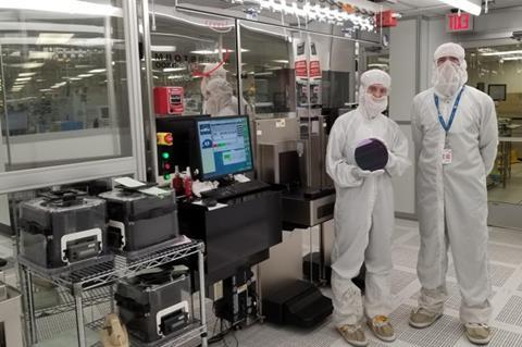
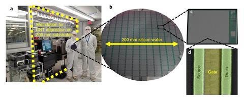
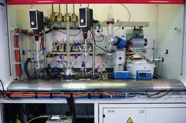
The new research uses incubation – a simple solution process widely used for making other types of transistor, but which had never been taken seriously for CNT transistors as the results are not quite as good as the very best achievable by other techniques. None of these more delicate methods, however, is practicable in industry. ‘For a long time, people – including us in our lab – were thinking we needed alignment, we needed the CNTs all super close together and specific distances apart,’ explains Bishop. ‘One of the big breakthroughs was realising that what we can do today can enable a lot of progress.’ Bishop and colleagues then optimised the incubation process for depositing CNTs. Simple innovations such as dry cycling, in which the silicon wafer is periodically removed and dried to stick the attached CNTs to the surface, reduced the production time from 48 hours to 150 seconds. The researchers then demonstrated nanotube transistor production independently at two commercial chip foundries.
The CNT transistors are not as good as the best silicon transistors yet, but the researchers believe that, after further development, the CNT transistors will ultimately prove superior to their silicon counterparts. ‘There’s research in the literature that, if you make the same 2D chip side-by-side but replace the traditional transistors with CNT transistors, the benefits are astronomical,’ says Bishop. ‘But it’s one thing to know those benefits could exist one day, and then there’s all the work to make it happen.’ Until then, the researchers believe scalable production of CNT transistors should enable them to scale-up circuits they have previously made that combine CNT transistors with traditional silicon ones.2
‘It’s very difficult to scale in the third dimension using existing silicon transistors, because they take over 1000˚C to build, so you destroy your bottom layer,’ Shulaker explains. ‘But the process that the team has developed is almost at room temperature, so we can build layers of CNT transistors directly on top of an existing CMOS chip,’ he adds. ‘We don’t need to beat silicon from day one: we can supplement it.’
‘It’s a nice blueprint for those of us who work with nanomaterials on how to take one of these technologies from the lab to a real-world situation,’ says electrical engineer Eric Pop of Stanford University in California, who was not involved in the research. He cautions, however, that the long-term stability and reliability of the devices still needs investigation. A crucial step, he says, is ‘building a 3D-based circuit that has advantages over a 2D circuit at industrial scale: otherwise the cost – which will go up – will not be worth it’.
References
1 M D Bishop et al, Nat. Electron., 2020, DOI: 10.1038/s41928-020-0419-7
2 M Shulaker et al, Nature 2017, 547, 74 (DOI: 10.1038/nature22994)


No comments yet