Atom-thin sheets of carbon are taking the materials world by storm. Richard Van Noorden discovers that now is the perfect time for chemists to join the party
Atom-thin sheets of carbon are taking the materials world by storm. Richard Van Noorden discovers that now is the perfect time for chemists to join the party
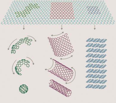
Unroll a nanotube and you will be left with a sheet of carbon, just one atom thick - the thinnest of all materials. Known as graphene, it is the latest star of 21st century materials science.

At one time it seemed impossible that planar graphene sheets could be studied in isolation. Chemists examined patches of carbon atoms attached to a surface as far back as the 1970s, but whenever carbon layers were prised from graphite, they would curve up or clump together. In 2004, however, Andre Geim, Kostya Novoselov and colleagues at the University of Manchester, UK, announced that by the simple method of cleaving graphite with sticky tape, they were able to view individual graphene flakes under an optical microscope.
The new material rapidly became the darling of theoretical physics. Thanks to the remarkable interactions of electrons passing through a two-dimensional honeycomb lattice, graphene has been used to demonstrate a number of surprising predictions of relativistic quantum mechanics. But it has practical potential too: suggested applications include sensors, transistors, terahertz imaging, composites, membranes, energy storage devices, batteries, and thin coatings for solar cells and LCD displays. Most tantalising of all, graphene may form the basis of a new breed of computer chips, smaller and faster than those based on silicon. And clever chemistry is starting to meet the challenges of graphene processing, moving the field beyond the academic playground of fundamental physics.
Physicists have used graphene to test some exotic predictions of quantum electrodynamics in the laboratory. This form of quantum mechanics describes how the movement of an electron is influenced by relativistic effects.
Electrons moving through an atomic lattice generally behave as if they were much heavier than normal, as they are pushed and pulled by the charges on other electrons and atomic nuclei.
But graphene’s charge carriers respond to electric fields as if they had almost no mass at all. They speed through the lattice a mere 300 times slower than the speed of light itself, thanks to the fortuitous interactions enabled by the symmetry of a 2D honeycomb lattice.
At these speeds, relativistic effects become important. Graphene’s charge carriers are best described, mathematically, like slightly sluggish, negatively-charged neutrinos.
One of the many exotic effects being investigated in graphene is the Klein paradox, which states that relativistic particles can pass through any potential energy barrier by temporarily pairing up with their antiparticles. In graphene’s case, this corresponds to electrons and holes passing through electric field barriers.
Making it big
Graphene’s lattice of hexagonally-arranged carbon atoms is remarkably free of defects or impurities. This pristine quality helps electrons shoot through the material for thousands of interatomic distances without scattering, and also helps to rapidly dissipate excess heat - making graphene a better-quality conductor than silicon. Not only could graphene-based transistors or circuits work faster than conventional silicon, they could also be smaller. Strong carbon-carbon bonds hold the sheets together even at sizes of a few nanometres, where silicon devices decompose or leak current.
With silicon computing expected to reach its limits in 15-20 years time, there’s intense interest in nanotube or graphene-based replacements. Major computing companies, such as Hewlett-Packard, IBM and Intel, are funding research into the area, while the EU-supported project GRAND (Graphene-based Nanoelectronic Devices) launched in January 2008.
One problem is that no-one has managed to create large enough sheets of graphene to pattern with conventional lithography. ’Scratching graphite is a great proof-of-concept method that gives high-quality graphene for laboratories - but it won’t work for industrial applications,’ says Geim.
The only commercial supplier of graphene is Graphene Industries, a spin-out company from the University of Manchester, UK. Because of the manpower needed to hunt for clean single-layer flakes (which involves peering through a microscope at differing colour contrasts on a silicon wafer), the service isn’t cheap: managing director Tim Booth says that flakes of a few hundred square micrometres sell for hundreds of pounds. Scaling these prices up means a theoretical square metre of clean graphene would cost ?500 billion, while to purchase a graphene quilt weighing a gram (and covering around three tennis courts) would require rather more than the US national debt.
A far cheaper method would be to deposit carbon atoms from a vapour onto an inert support. But that process is already used to produce nanotubes commercially: the carbon atoms tend to curl up around impurities, rather than remaining as sheets. Still, researchers such as Johann Coraux, at the University of Cologne, Germany, have recently shown that high-quality graphene can be deposited on metal surfaces, such as iridium - and are now hoping to transfer these layers onto insulating wafers. Walt de Heer’s group at the Georgia Institute of Technology, Atlanta, US, have another method: heating silicon carbide in a vacuum so that the uppermost silicon atoms escape, leaving behind graphene layers.
Transistor tinkering
De Heer, Geim, and a team led by Max Lemme at the electronics company AMO in Aachen, Germany, have already claimed the first proof-of-concept graphene transistors, which can be used to switch current on and off (see Chemistry World, April 2007, p25). In one type, a variable electric field is used to control current flow through a graphene sheet. In another model, two graphene ribbons surround a central quantum dot, also made from graphene, which similarly restricts the passage of electrons. The problem is that graphene is too good a conductor, persistently letting electrons through when the current is meant to be off. As Geim puts it, ’graphene transistors leak like hell’.
Sculpting some parts of a graphene circuit into very narrow (5-10nm diameter) ribbons may help. This trick changes the material’s electronic properties from metal to semiconductor, by confining the lateral movement of electrons and opening up a band gap. In principle, a whole circuit could be made from graphene sculpted to different widths, though reliably etching to such fine resolutions may be beyond the limits of lithography.
These intrinsic difficulties, says Phaedon Avouris, who researches nanoscale electronics at IBM’s T J Watson Centre in New York, US, mean that researchers may be better off avoiding logic devices, and focusing instead on the advantages of electron mobility. Wavelengths of electrons speeding through graphene could reach the much sought-after terahertz range, for example, allowing high-frequency terahertz wave imaging of the kind used in security scans and medical imaging (see Chemistry World, March 2007, p52).
Calling all chemists
Ingenious chemical patterning may spring to graphene’s aid, however. ’The chemistry part of the graphene story has only just begun,’ says Rod Ruoff, who works at the University of Texas in Austin, US.
Ruoff hopes that molecules can be called in to bind to graphene’s edges or surfaces, and alter the material’s electronic properties. If hydrogen could be deposited onto channels of carbon atoms, creating stripes of tetrahedral (non-conducting) carbon atoms that confine a conducting core, there would be less need for tricky lithography.
So-called ’chemically modified graphene’ (CMG) has not reached this level of sophistication yet - although a collaboration between Geim and Lemme’s Aachen team has resulted in a pre-print paper suggesting that hydrogen and hydroxyl ions binding reversibly to graphene could turn its conductivity off and on, making an electrochemical switch.
The most useful chemical decoration of graphene so far has involved splitting graphite into individual CMG sheets. Ruoff’s group showed in 2006 that graphite oxide, unlike graphite, readily falls apart in solution as oxygen atoms repel water molecules. This gives graphene oxide sheets, which his team are now depositing onto substrates and converting back to conductive modified graphene.
In January 2008, meanwhile, Australian researchers led by Dan Li at the University of Wollongong, New South Wales, used a sequence of chemical reactions on graphite oxide to produce well-dispersed graphene sheets in solution; and in the same month, Hongjie Dai and colleagues at Stanford University, US, announced a chemical alternative to lithography for making 10nm-wide smooth graphene ribbons, by bathing graphite in hydrogen and argon at high temperatures, before shaking it apart with ultrasound.
But there’s certainly room for improvement. ’Oxidation of graphite . inevitably introduces defects into the graphene, because of the formation of oxygen-containing groups,’ explains Klaus M?llen, who works at the Max-Planck Institute for Polymer Research in Mainz, Germany. His group is attempting to synthesise graphene from its constituent benzene rings - a difficult task, though it guarantees high purity. In March 2008, M?llen reported that by coupling aromatic rings together, his team had produced graphene nanoribbons up to 12nm long, which dissolved in organic solvents.
Future-proofing
Chemists won’t be too concerned if their alternative approaches to graphene don’t immediately bear fruit in electronic circuits. They are turning their attention to other exciting applications, much closer to commercial realisation. Soluble graphene sheets can easily be sprayed or filtered to create a thin transparent conductive coating, for example, suitable for LCD screens. M?llen’s team, citing a worldwide shortage of indium (which is used to make indium tin oxide (ITO) electrodes for LCDs and solar cells) has focused efforts on making transparent electrodes from graphene.
Ruoff’s group, meanwhile, has encapsulated CMG sheets in polymers and silica glass to make strong composites, and last year weaved graphene oxide into extremely strong, but thin, paper. The bonus of all these applications, Manchester’s Kostya Novoselov notes, is that the graphene doesn’t have to be anywhere near the quality required for electronic circuits - in fact, graphene powder can be quite cheap to produce.
Nanotubes in disguise?
With prospective applications including gas sensors, batteries and capacitors, as well as composites and electrodes, the buzz around near-term applications for graphene seems rather familiar. Researchers, unsurprisingly, are casting around in the same kinds of fields where carbon nanotubes have shown promise. Nanotubes are, after all, simply graphene sheets folded up - so why not use them instead?
For electronic circuits, nanotubes have several difficulties which graphene may overcome. They’re hard to produce with a well-defined size and conductivity and, since they’re not flat sheets ready to be sculpted, connecting tubes up into circuits can produce high resistance junctions. But as Avouris warns, ’Graphene is not a panacea for every application.’
Graphene’s flatness means it has a large surface area to volume ratio. That makes it, perhaps, a slightly better candidate for anything requiring absorbing atoms or ions. Ruoff also speculates that it could be rolled up into a ’Swiss-roll’ style capacitor. Combining this surface area with high conductivity means that any molecular disruption on the sheet is easily detected, and Geim’s team has shown that graphene is so sensitive it can count individual gas molecules on and off its surface at room temperature (see Chemistry World, September 2007, p29). ’Depending on the particular problem in hand, graphene’s prospects can be sometimes superior, sometimes inferior, and most often completely different from those of carbon nanotubes,’ Geim summarised in a recent review article.
The odds of success
Wary of overhype, Geim cautions that the prospects of graphene becoming the next silicon are at least 20 years distant - and still a huge experimental goal. ’The nearest niche applications are those for computer screen coatings or ITO electrodes , perhaps three years away,’ he says.
It’s salutary to remember, too, that graphene is not the only 2D crystal in town. Novoselov points out that boron nitride and chalcogenides are among the flat, atomically-thin materials created since 2004. What’s more, the emphasis on single layer graphene may be unwarranted. Avouris and other researchers are now investigating the properties of two or even more layers of carbon sheets (it takes about 10 layers before the electronic properties revert to those of graphite).
’Whatever happens, we know graphene is unique, and will be around for several decades. It has at the very least opened up a wealth of new physics,’ Geim concludes. Indeed, it is theoretical physicists who have had most fun with graphene so far. Time for chemists to join the party.
Further Reading
K S Novoselov et al, Science, 2004, 306, 666 (DOI: 10.1126/science.1102 896)
P Avouris et al, Nature Nanotech., 2007, 2, 605 (DOI: 10.1038/nnano.2007 300)
A K Geim and K S Novoselov, Nature Mater., 2007, 6, 183 (DOI: 10.1038/nmat.1849)
L Zhi and K M?llen,J. Mater. Chem., 2008, (DOI: 10.1039/b717585j)
R Ruoff, Nature Nanotech., 2008, 3, 10 (DOI: 10.1038/nnano.2007, 432)
D Li et al, Nature Nanotech., 2008, DOI:10.1038/nnano.2007.451


No comments yet