New technique allows large scale production of defect free graphene suitable for electronics
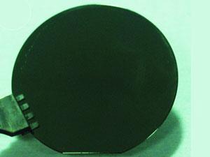
Macroscopic films of monolayer, single crystalline graphene free of the defects that dog other production methods have been grown on germanium. The technique makes it possible to grow large sheets of single crystalline graphene, potentially allowing applications that aren’t possible presently.
Graphene is famed for its remarkable flexibility, strength and, above all, electronic properties. This makes graphene a potential replacement for silicon in next-generation electronics. But the mechanical exfoliation or ‘Scotch tape’ method for producing crystalline graphene, in which micrometre-scale flakes of graphene are painstakingly extracted from bulk graphite, is inconvenient and useless for industry.
Chemical vapour deposition, however, can produce large graphene sheets. In this process, a carbon-containing gas such as methane is passed over a copper substrate. Graphene crystals nucleate at multiple points and grow together into a single sheet. Unfortunately, copper is inherently polycrystalline and atomically rough, which gives the graphene crystals variable orientations. When the crystals join up, therefore, defective grain boundaries and wrinkles form. These both scatter electrons, which can significantly reduce conductivity. Furthermore, the copper has to be etched away with acid, and disposal of this can pose environmental hazards.
Dongmok Whang and colleagues at Sungkyunkwan University and the Samsung Advanced Institute of Technology, both in Korea, replaced copper with germanium. When methane gas and hydrogen were passed over the germanium, graphene crystals all grew with the same orientation, before joining together into a single crystalline sheet of graphene in which no defects or wrinkles could be detected. The graphene could be removed simply by placing gold film over the top and pulling it off, allowing the germanium wafer to be used over and over again.
Nanoscientist Jiwoong Park of Cornell University, US, is intrigued. He says the electron mobilities measured by the researchers are lower than the very best figures quoted for polycrystalline graphene, although he suspects this may arise from differences in the way the mobilities were measured. He believes, however, that the work has other potential. ‘People are now studying two-layer and three-layer graphene systems where each layer has a different orientation,’ he says. ‘I think the current paper is excellent for stacked materials because you can control the orientation of each layer perfectly.’ Graphene pioneer Rodney Ruoff of Ulsan National Institute of Science and Technology in Korea agrees the control of orientation is ‘an important scientific achievement’. ‘It’s a material that now needs to be worked with and tried in different applications,’ he says.
The researchers are now looking at thin strips of graphene – nanoribbons. ‘The properties of nanoribbons strongly depend on the crystal orientation,’ says Whang. ‘I believe we can fabricate wafer-scale arrays of the nanoribbon devices with uniform characteristics.’




No comments yet