First ever synthesis of stanene will give scientists the opportunity to see if its electronic properties are as odd as predicted
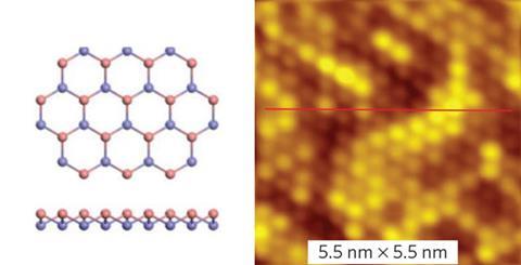
Until now, the production of stanene has proved elusive. ‘Bulk tin with a diamond structure is not a layered material,’ explains one of the team’s leaders, Jin-feng Jia, of Shanghai Jiao Tong University in China. ‘Free-standing stanene may not be stable; in order to get stanene firstly one must have a suitable substrate, secondly one has to determine that the film has the necessary honeycomb-like bilayer atomic structure, and thirdly one has to determine that the film has the right electronic band structure. All the experiments have to be done in situ in an ultrahigh vacuum system.’
A key to the success of the new work was to identify a suitable substrate upon which to condense highly purified tin atoms by molecular beam epitaxy under tightly controlled conditions. The researchers found that bismuth telluride (Bi2Te3) fitted the bill as a substrate. ‘Stanene has a hexagonal lattice, so the surface of the substrate must also have a hexagonal lattice,’ says Jia. ‘The lattice mismatch between the substrate and the stanene should be small and it should be energetically favourable to stanene to grow in a quasi-two-dimensional growth mode on the substrate.’
The researchers grew a layer of tin atoms on the substrate and confirmed its predicted structure – resembling buckled honeycomb – through scanning tunnelling microscope imaging. Key electronic characteristics were measured using angle-resolved photoemission spectroscopy. ‘With the help of first principle calculations our experimentally determined atomic and electronic structures agree with the theoretical predictions,’ Jia says.
Having created what they are convinced is stanene, the team says that the next task will be to carry out electronic transport measurements to explore the potentially unusual quantum properties that have been predicted for the material.
Commenting on the study, Neil Wilson, who works on two-dimensional materials at the University of Warwick in the UK, says: ‘This is a crucial first step in exploring the properties of this new material, but there are still significant challenges. Here the growth substrate interacts strongly with the stanene, fundamentally changing its properties. It will be necessary to isolate the stanene from the growth substrate in order to test its intrinsic properties against the theoretical predictions. Applications will then require integration of the stanene with other materials, without losing its intrinsic properties.’
Correction: On 10 August the story was updated to include the correct formula for bismuth telluride


No comments yet