Flexible electronics are destined to transform the way we manufacture and interact with electronic devices. Graphene’s high electrical conductivity and mechanical stability could prove beneficial in flexible electronic circuits. However, despite its potential, graphene is typically only produced and patterned in research environments with economic barriers hampering its use in commercial applications.
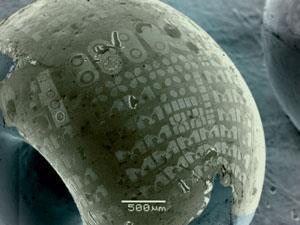
Now, a group led by Mario Hofmann at National Cheng Kung University have demonstrated an easy and scalable approach to depositing high resolution graphene patterns onto surfaces. Fabrication begins by ink-jet printing an aluminium chloride layer onto copper foil – the aluminium chloride layer acts like a template for graphene growth by chemical vapour deposition. A thin polymer membrane is then added to support the patterned graphene when the aluminium chloride is removed and whilst it is transferred from the copper foil to the desired surface. In contrast to conventional crystalline semiconductors, the graphene pattern can be transferred onto complex 3D substrates. ‘Graphene’s atomic thickness makes it ideally suited to conform to 3D surfaces,’ says Hofmann. ‘The target substrate can be of any shape and does not need to be compatible with the deposition process.’
Mark Hersam, an expert in nanoscale materials at Northwestern University in the US, praises the work as ‘a clever strategy for achieving patterned graphene growth with the possibility of low cost manufacturing and compatibility with flexible substrates’. He adds that the work represents an interesting advance for the graphene field, but that issues remain in using this material for electronics due to the absence of a band gap.
Hofmann’s team hope to extend their work by producing complete circuits on curved surfaces which could be used in ‘smart’ glasses and wristwatches.


No comments yet