Fabrication methods combining printing and lithography have proven fertile. Andy Extance now asks how successful will they be outside the lab
Fabrication methods combining printing and lithography have proven fertile. Andy Extance now asks how successful will they be outside the lab?
But what if photolithography hits a barrier it cannot breach? That question has motivated scientists to recruit chemistry to a series of printing methods with the power to engineer nanometre-scale materials. These approaches are also far more affordable and accessible for those outside the electronics industry. Therefore, while conventional chipmaking powers on, these methods enable nanoscale research and manufacturing in a way that has never been seen before. Yet one major question remains: can they become tools – like photolithography – whose relevance is embedded in our society? Or will their role beyond academia be limited?
The challenges facing the electronics industry, both familiar and quite different, provided one motivation for Harvard University’s George Whitesides to first look at other methods for nanofabrication. ‘In the 1980s there really was a concern that photolithography was going to run out of steam,’ he recalls. ‘People thought it would be hard to go below 1µm, which now seems ridiculous.’ Whitesides also wanted to give those outside the electronics industry the opportunity to work with nanostructures, without needing ultra-clean conditions.
Fine print
Today, mainstream photolithography begins when a worker applies polymeric photoresist to a metal or semiconductor. They align a patterned mask over its surface, and change the solubility of the photoresist in exposed areas through reactions triggered by a laser. The engineer can then develop the resist, washing unreacted material away. That leaves exposed areas of metal or semiconductor to be etched away by treatment with chemicals, such as buffered hydrofluoric acid, or plasma. Finally, the worker removes the polymer resist to get the structure they want.
Telecoms equipment maker Lucent Technologies was an early beneficiary of soft lithography’s capabilities, when John Rogers moved from Whitesides’ group to its renowned Bell Labs in Murray Hill, New Jersey in 1997. Using soft lithography to make circuits on the outside of optical fibre, Lucent produced devices to reduce error rates in light signals travelling over long distances. But after the dot-com bubble burst, Rogers faced the stark realisation that he could not push the techniques as far as he wanted at a shrinking Bell Labs.
Getting flexible working
Rogers wanted to make higher performance flexible electronics than would be allowed by the comparatively poor capabilities of the organic semiconductors from which they are often made. ‘If you could print silicon, that would provide much higher functionality, more robust operation, higher performance,’ he explains. So when he moved to his current lab at the University of Illinois in Urbana-Champaign, US, in 2003, Rogers turned to transfer-printing ribbons of inorganic semiconductor tens of nanometres thick.
Transfer printing stamps must always pick up their target, and also always drop it at its destination. To control pick-up adhesion, silicone stamps can be modified with methyl groups to make them more hydrophobic, or oxidise them to increase their hydrophilicity. Reactive chemical or adhesive anchors at the destination can then ensure the target – such as a semiconductor ribbon – leaves the stamp. ‘The strength of the adhesion depends on the rate at which you peel the stamps away,’ Rogers adds. ‘You can control with rate, contact force, and surface chemistry – there’s a host of strategies.’2
Meanwhile, Grant Willson of the University of Texas in Austin, US, had different silicon-focused nanoscale printing ideas, for the mainstream semiconductors used in processor chips. When working at IBM’s Almaden labs in California around 1990, Willson wondered if rapid, high resolution, imprinting of information onto optical computer discs could be adapted to produce such structures. He realised that while soft lithography was versatile and cheap, it could not be used for this purpose. ‘The template is an elastomer and therefore aligning layers at nanometre level precision over large areas seemed very problematic,’ Willson says.
Another possibility, known as nanoimprint lithography, uses hard templates to print patterns in resist material that is made fluid by heating. Though it required fewer process steps than optical lithography, Willson knew cooling and hardening the resist would take too long for chipmakers. Willson therefore used experience gained developing ‘chemically amplified’ photoresist polymers at IBM to invent a process with rapid light-triggered resist patterning, known as step-and-flash imprint lithography, or SFIL.3
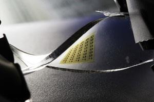
Technology giant Hewlett-Packard (HP) has been developing its own imprint lithography process, motivated by a similar interest in optical discs and the power of UV polymerisation. It wants to make flexible displays that fly off a roll-to-roll production line much like a newspaper might. But that is a tall order, demanding the accurate patterning and positioning of several electronic and optical layers on a plastic film that could be easily distorted in optical lithography, destroying critical alignments.
On display
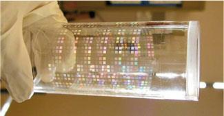
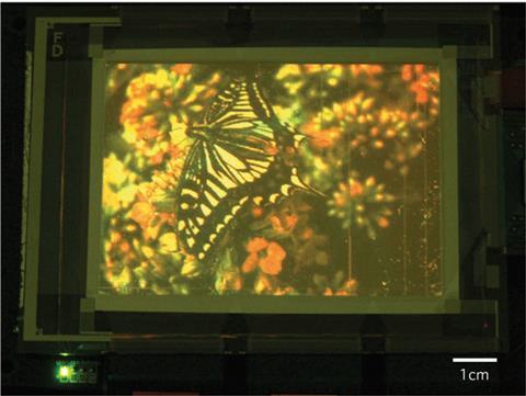
After imprinting the resist, the HP team can shine UV light through the roller and solidify the pattern just after the stamp touches the film roll. The researchers can then etch through one layer of display material, but only etch away a certain depth of the resist. That removes some parts of the pattern, but leaves others that are needed to mask the next layer of electronic material. The etching continues, alternating between display and mask, with careful selection of selective etching chemistry. The process retains alignment for feature sizes below 100nm in spite of any film distortion, and HP has already used it to produce prototype flexible displays.
Transfer printing may also be used to make displays by building up rather than etching away layers, according to Jong-Min Kim of the University of Oxford, UK. As senior vice-president and director of Samsung Electronics’ Frontier Research Laboratory in Yongin, Korea, he was responsible for developing displays made up of quantum dots. These nanometre-scale semiconductor particles emit light when a voltage is passed through them, with their colour dependent on their size. With these properties, they could replace several layers of colour filters and liquid crystals. However, with these displays in their early stages, precise ways to pattern them had been elusive.
Imprint impact
Taussig underlines that HP’s SAIL technology is near pilot production, with the company focusing on increasing manufacturing yields and producing larger area backplanes. ‘The remaining chemical challenges are in the polymer substrates,’ he explained. ‘They need to be cleaner and more stable.’ Nevertheless, the HP executive thinks the technology could be revolutionary. ‘In my opinion, roll-to-roll manufacturing with imprint lithography will enable an incredible disruption in the electronics industry,’ he says. ‘Eventually we will see rollable or foldable displays. In a few years, glass displays will seem as anachronistic as cathode ray tubes seem today.’
In 2001, Willson backed his imprinting approach by founding Molecular Imprints to supply SFIL equipment to manufacturers. Today such tools are helping develop the next generation of hard disk drives, which store data in bits too small for previous manufacturing tools. ‘These dots have 10nm-scale dimensions and nothing else can print it,’ Willson said. His team has also shown that SFIL could improve the processes currently used to form copper wiring on integrated circuits by reducing the number of steps involved from 184 to 64.Eventually we will see rollable or foldable displays
Yet many such nanoscale printing approaches are still at pre-commercial stages. Even worse, as processor chip makers look to shrink their transistors below 22nm, they continue to back optical lithography. The likes of Samsung and Intel paid toolmaker ASML €1.38 billion in 2012 to develop tools that use extreme ultraviolet (EUV) wavelength lasers needed for smaller transistors. That frustrates Willson. ‘Semiconductor companies are giving money to EUV lithography, but it keeps missing all of its deadlines,’ he says. But having already contributed one important technology to the semiconductor industry, Willson remains positive that SFIL could come to the rescue. ‘I remember trying, with difficulty, to imagine a time when most patterning would be done with chemically amplified resist,’ he said. ‘As I speak to you, virtually every part is made with this material.’
Fabricating a future
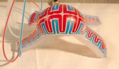
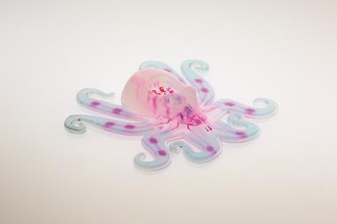
And, having shown that soft lithography can make features as small as 2nm, Rogers’ team is also using its various techniques to devise products that did not exist before. These include bio-integrated electronic devices, combining hard mono-crystalline silicon with soft silicone polymer. His team is developing clinical monitors for attachment to heart, brain and skin, and Rogers has also founded a spin-out company called MC10 looking at more short-term commercial opportunities. ‘They have a joint development arrangement with Reebok to put monitoring electronics into athletes’ clothing,’ Rogers says. ‘They’re very close to launching their first product.’
Rogers and Whitesides have also co-founded photovoltaic module producer Semprius in Durham, North Carolina, US, which opened a pilot manufacturing plant in September 2012. Their modules use lenses to focus sunlight on tiny, highly efficient, cells precisely assembled by transfer printing. Other companies have also produced such ‘concentrating photovoltaics’, with mixed outcomes. But this year Semprius set a world record for module efficiency, reaching 33.9%.
Though Rogers is cautious about these technologies’ chances, he underlines that commercialisation would be the biggest validation of transfer printing. ‘We judge ultimate success by whether technologies can be beneficial outside the academic context,’ he says. ‘We’re optimistic it’s going to work.’
Andy Extance is a science writer based in Exeter, UK
References
1 D Qin et al, Nat. Protocols, 2010, 5, 491 (DOI: 10.1038/nprot.2009.234)
2 A Carlson et al, Adv. Mater., 2012, 24, 5284 (DOI: 10.1002/adma.201201386)
3 C G Willson, J. Photopolym. Sci. Technol., 2009, 22, 147 (DOI: 10.2494/photopolymer.22.147)
4 H-J Kim et al, J. Soc. Inf. Display, 2009, 17, 96 (DOI: 10.1889/JSID17.11.963)
5 T-H Kim et al, Nat. Photonics, 2011, 5, 176 (DOI: 10.1038/nphoton.2011.12)


No comments yet