
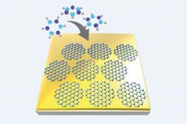
Molybdenum diselenide layer mirrors could have optoelectronic applications
Optoelectronics, in which photons interface with electrons to carry information within and between circuits, is a growing field many physicists believe will be crucial to increase computers’ power. Essential to its advancement are atomic-scale technologies to manipulate photons within optical integrated circuits. Now, two research groups – one in Switzerland and one in the US – have simultaneously developed atom thick mirrors that can be switched electrically.1,2
Semiconductors are generally transparent to photons with energies below their band gap – the energy required to promote an electron from the valence band to the conduction band, leaving a positive ‘hole’ in the valence band. However, the energy a photon needs to create an electron–hole pair or exciton is lower than the energy needed to create a free electron and hole. In most materials, this energy difference is small, but in transitional metal dichalcogenides such as molybdenum diselenide, it can be around 0.5eV, giving the materials a strong absorption peak in a wavelength region in which the material is otherwise transparent.
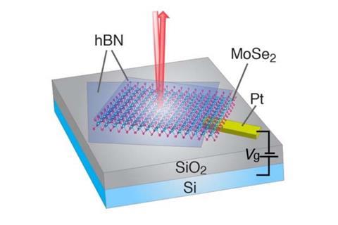
Under normal circumstances, these excitons predominantly decay by losing their energy to the lattice as heat. However, researchers at Harvard University and colleagues in Japan, as well as – independently – researchers at ETH Zurich, made an interesting discovery. In monolayer molybdenum diselenide cooled to 4K and encapsulated by monolayers of the dielectric hexagonal boron nitride excitons can decay by re-emitting a photon. By engineering their devices to strongly favour emission in the backward direction, the groups created atomically-thin mirrors
Furthermore, by reducing the voltage on the molybdenum diselenide the reflectivity could be switched on and off electronically. ‘One could in principle switch this on tens of gigahertz to hundreds of gigahertz timescales,’ says ETH Zurich’s Martin Kroner, ‘That could be very interesting for integrated optoelectronics.’ Nevertheless, significant issues remain. ‘If you always have to work at 4K, it’s not good, obviously, except for some niche applications,’ explains Harvard’s Hongkun Park. ‘Even with our preliminary structures, the reflectivity survives up to 150K. If you improve the material properties, you might even go all the way up to room temperature.’
‘It’s definitely work that’s seen as a big milestone in this field,’ says Frank Koppens of the Institute of Photonic Sciences in Spain. The low-temperature requirement makes him sceptical of widespread use in optoelectronics, but he says there may be real potential for manipulating photons in quantum information processing. ‘In that field, low temperature is considered a given and not a major roadblock,’ he says. Ultimately, he adds, ‘this is a big step forward in terms of the quality of these materials. We should not immediately run into all these discussions about applications because it’s very hard to predict the applications new materials can offer.’
References
1 P Back et al,Phys. Rev. Lett., 2018, 120, 037401 (DOI: 10.1103/physrevlett.120.037401)
2 G Scuri et al,Phys. Rev. Lett., 2018, 120, 037402 (DOI: 10.1103/PhysRevLett.120.037402)


No comments yet