
A method for growing graphene-like films with precisely engineered defects offers a new route to tailor the material’s properties for specific applications.
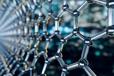
Defects are often undesirable in materials like graphene. But in certain cases, they can actually enhance its chemical, electronic, mechanical and magnetic properties.
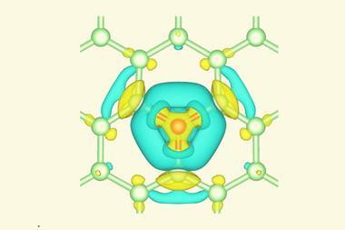
Now a team led by Reinhard Maurer from the University of Warwick, UK, and David Duncan from the University of Nottingham, UK, has developed a one-step chemical vapour deposition (CVD) process to introduce defects directly during growth. It employs azupyrene, a precursor molecule designed to mimic the topology of a Stone–Wales defect by including two pentagons and two heptagons where there would normally be four adjacent hexagonal rings. These other rings influence the material’s interactions with substrates and modifies its electronic and magnetic behaviour.
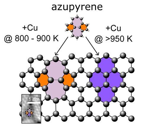
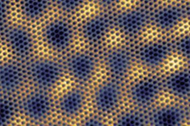
By growing carbonaceous films on copper substrates at varying temperatures, the researchers were able to control the concentration of these five- and seven-membered rings. The team used advanced microscopes at Diamond Light Source in the UK and MAX IV in Sweden to study the atomic structure of the defective graphene. Higher temperatures produced structures closer to pristine graphene. Importantly, the resulting monolayers were continuous and not contaminated with heteroatoms, an improvement over post-processing methods of graphene oxide or pristine graphene that can result in defect inhomogeneity and unwanted impurities.
The work opens new possibilities for graphene with engineered defects in areas such as nanoelectronics, gas sensing and catalysis, where controlled reactivity and electronic behaviour are essential.


No comments yet