
Well-ordered semiconducting graphene with a bandgap has been grown on the surface of silicon carbide by researchers in China and the US. The team was then able to make use of this unusual combination of properties in graphene to produce a transistor. The work could lead to direct integration between silicon electronics and high-power circuitry.
Physicists have for years attempted to put the remarkable electronic mobility of graphene to use in next-generation electronics, but have been persistently hamstrung by the complete absence of a bandgap. This means that in the transistor – the fundamental component of the digital electronic circuit – the current would flow incredibly fast in the on state, but would be impossible to turn off. They are therefore experimenting with other 2D materials such as molybdenum disulfide that have bandgaps, but much lower electronic mobilities.
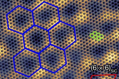
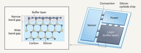
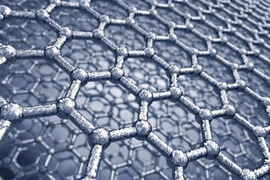
Silicon carbide has a bandgap around 3eV. When it is heated to high temperatures, some of the silicon atoms sublimate, leaving a layer of ‘epigraphene’ on the surface. This has a narrow 0.6eV bandgap because of interactions with the substrate. Unfortunately, it normally has very low electronic mobility because the missing silicon atoms underneath lead to a disordered bonding environment. ‘You have to have a periodic structure in order to support this semiconducting property – it’s a very fundamental property of materials,’ says Walt de Heer of Georgia Institute of Technology in the US. ‘If you make the material more ordered you get a better-defined bandgap and your mobilities go up.’
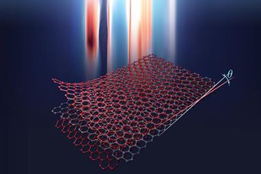
De Heer and colleagues led by Lei Ma at Tianjin University in China developed an alternative technique where two silicon carbide chips are placed parallel to each other, with the silicon plane of one facing the carbon plane of the other. When they heated the system, silicon atoms sublimated from the silicon face and formed a film on the carbon face. Carbon atoms displaced from the carbon face were transferred to the silicon face, where they formed a well-ordered, evenly bonded layer of epigraphene with a room-temperature electronic mobility 10 times that of silicon, 20 times that of other 2D semiconductors and 5500 times greater than conventionally produced epigraphene. When the researchers integrated their material into a transistor, they found that electronic mobility dropped by a factor of 200. They believe this is because other elements of the structure were not optimised and they are now working to do so.
Andrea Ferrari at the University of Cambridge’s Graphene Centre is sceptical that the work will have significant value for post-silicon electronics. ‘The problem is that this semiconducting graphene only exists because of the bonding that exists on silicon carbide between the buffer layer and the substrate,’ he says. ‘The moment you try to peel it off it will mostly recover its original properties so it will not be [a semiconductor].’ He adds, however, that interest in wide-bandgap semiconductors like silicon carbide is ‘truly exploding’ thanks to its importance in devices like electric vehicles, but silicon carbide is not directly integrable with silicon. This work, he says, shows ‘what the future could look like’.
De Heer, however, is convinced their epigraphene could be valuable in electronics. ‘We’ve a paper we wrote years ago on how to integrate graphene with silicon using the well-established silicon-on-insulator technique,’ he says. ‘You take an extremely thin silicon layer and you lay it on top of the graphene layer, so you have silicon electronics on the top basically controlling the graphene, and below all that is silicon carbide.’ This, he says, could allow them to exploit the advantages of epigraphene to go beyond silicon without needing to remove it from the substrate.
References
J Zhao et al, Nature, 2024, 625, 60 (DOI: 10.1038/s41586-023-06811-0)


No comments yet