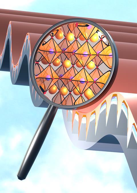
Clever structure boosts efficiency and cuts production costs
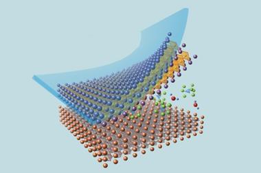
Researchers have developed flexible back-contact perovskite solar cells using a process directly scalable to large-area, low-cost manufacturing. The innovative design features micro-grooves embossed into a plastic substrate, created using techniques compatible with roll-to-roll processing.
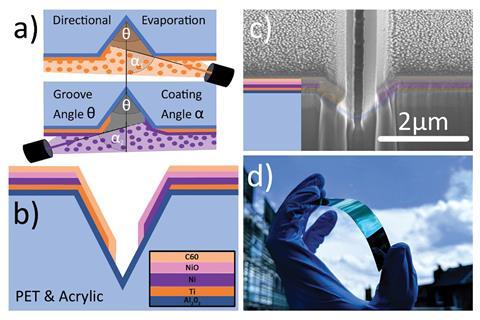
Back-contact solar cells have an active layer directly exposed to the illumination source, reducing parasitic absorption and reflection losses. This architecture also allows the cells to feature non-transparent, yet highly conductive, metal electrodes. Previously, back-contact perovskite solar cells could only be made using time-consuming patterning techniques such as electrodeposition. Now, David Lidzey and co-workers at the University of Sheffield, UK, in collaboration with the company Power Roll, have designed interdigitated back-contact cells that are much simpler to build. The cells are paper-thin, lightweight and free from rare earth metals, and the team connected them to create micro-modules – the first time that researchers have arranged back-contact perovskite solar cells in such a way.
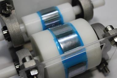
The fabrication process has several steps. First, the team embossed V-shaped micron-width grooves into a polymeric substrate. They deposited different, evaporable charge-selective contact materials onto opposing walls of the grooves by rotating the substrates, and then filled the grooves with perovskite via spin coating, forming devices with the multilayer structure Ti/C60/CH3NH3PbI3/NiO/Ni. Less than 2 microns separate the device contacts: ‘This spacing helps reduce electrical losses within the device due to charge–carrier recombination,’ explains Lidzey.
The devices had a maximum power conversion efficiency of over 7%, a record for interdigitated back-contact perovskite solar cells. Lidzey says the ease of interconnection between adjacent grooves is one of the really big benefits of the devices. ‘We have recently made larger modules, containing multiple cascades of grooves, with around 3000 grooves patterned over an area of around 4cm2.’ The team next aim to produce multiple device cascades over a 100cm2 area, and to explore different perovskite formulations to boost the cells’ stability amongst other improvements.
Neil Spann, managing director of Power Roll, says the solar module will weigh less than 0.5kg/m2, ‘which is six times lighter than other flexible solar photovoltaic modules and 24 times lighter than traditional silicon photovoltaic modules.’ Lighter devices mean lower transport and installation costs, and Spann anticipates the modules could be deployed where existing photovoltaic technologies cannot, for example on non-loadbearing rooftops and curved surfaces.
‘Among the many advantages of this configuration is the possibility to eliminate one of the most expensive components of a perovskite solar cell, the transparent conducting oxide electrode,’ comments Mónica Lira-Cantú, a solar cell expert at the Catalan Institute of Nanoscience and Nanotechnology, Spain. She envisages that this architecture ‘will impact the development of perovskite solar cells in novel applications where the use of the transparent conducting electrode is not always favourable, or on special substrates which don’t facilitate the fabrication of smooth and pinhole-free thin films, for example, in wearables or for the internet of things.’
References
This article is open access
M Wong-Stringer et al, Energy Environ. Sci., 2019, DOI: 10.1039/c8ee03517b


No comments yet