Manipulating MXene layers delivers the first semiconductor in the family
Scientists in the US have discovered a new way to tune the electronic properties of 2D MXene materials – by switching up the metals in the outer layers. As a result, they have created the first semiconducting MXene.
2D materials have come into their own over the past decade, with chemists and engineers taking advantage of their exceptional properties to make miniature electronic devices, store electrochemical energy or purify water. Among them graphene has so far received the most attention, but single-element materials are inherently unable to offer the same diversity in properties as those made up of two or more elements.
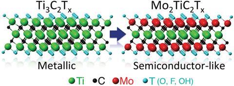
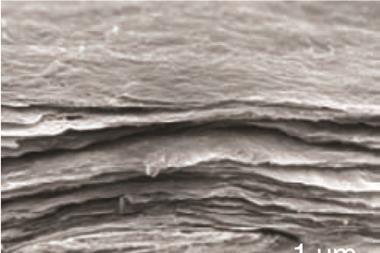
In 2011, Yury Gogotsi from Drexel University and co-workers discovered a new family of materials that host two to four layers of a transition metal interlaced with layers of carbon, and termed them MXenes. Researchers have made around 20 examples, some of which have already shown promise as electrodes for supercapacitors and aqueous batteries as they offer a unique combination of metallic conductivity and hydrophilicity.
‘Until now only metallic MXenes have been experimentally reported, so similar to the situation for graphene, opening the band gap has become an urgent research task,’ comments materials scientist Qian Wang from Peking University, China. Indeed, tuning the band gap could furnish semiconducting MXenes, which could prove to be useful transistors for electronic and sensing applications.
While doping and surface functionalisation are the typical go-to tools when it comes to modifying a material’s electronic properties, Gogotsi’s team now report an unprecedented strategy to do so. They replaced the outer two layers of a titanium-based material with molybdenum, and owing to changes in the electronic structure, they found that their multi-metal material exhibits semiconductor-like behaviour. Not only is this level of atomic control impressive, especially on a material that’s less than one nanometer thick, but their method should open the door to a whole range of new materials with diverse properties.
‘We are now trying to expand the MXene family and understand how the properties change as we modify the elements, the surface termination and the number of atomic layers in the structure,’ says Gogotsi. ‘This should give engineers a large variety of 2D materials to choose from for whatever devices they wish to develop. We want to give the community a new family of materials that will provide building blocks for the technology of the future.’
References
This article is free to access until 20 April 2016
B Anasori et al, Nanoscale Horiz., 2016, DOI: 10.1039/c5nh00125k


No comments yet