Super hard two-dimensional allotrope has electronic properties that make it a good match for graphene in transistors
The first two-dimensional form of boron has been synthesised by researchers in China.1 The super hard material, which was formed by two-stage chemical vapour deposition, has unusual properties for a two-dimensional material that could potentially make it very useful in nano-electronics – it is an air-stable semiconductor with a direct band gap.
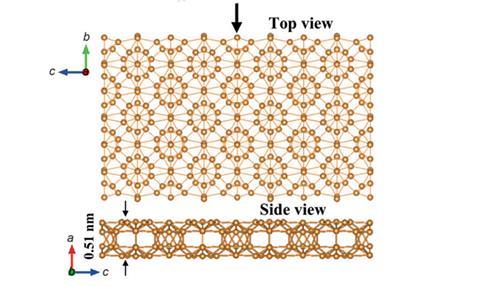
The bonding in bulk boron is very strong and yet highly complex and delocalised, and cannot properly be classified as ionic, covalent or metallic. It has at least 16 known polymorphs that exist at different temperatures and pressures. However, no two-dimensional forms of boron have been created, and researchers have debated what such a polymorph would look like. Whereas graphene is simply a single layer of graphite, there exists no planar form of bulk boron from which a single layer could conceivably be exfoliated.
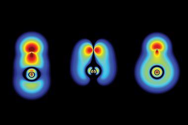
In the new research, Guoan Tai and colleagues at the Nanjing University of Aeronautics and Astronautics in China used a homemade two-zone chemical vapour deposition furnace. In the first zone, held at 1100°C, they combined boron and B2O3 powder to create B2O2 vapour; they then fed this into the second zone, held at 1000°C, where they reduced it with hydrogen and passed it over copper foil. This resulted in the formation of a polycrystalline monolayer comprising B12 icosahedra held together by B2 dumbbells. Intriguingly, negative charge moves away from the dumbbells onto the icosahedra, effectively making the molecule a boron boride.
Further analysis revealed that the material, a two-dimensional analogue of a high pressure phase called ?-B28, is a semiconductor with a sizeable direct band gap. This could make it useful for combination with graphene, because graphene’s lack of a band gap makes it difficult to create an ‘off’ state for nano-electronic devices. ‘2D boron can be extensively applied in future optoelectronic devices and transistors,’ says Tai. ‘More importantly, the 2D boron will be used in high temperature devices and nano-electromechanical systems owing to its high chemical stability and exceptional mechanical properties.’
Electronic structure theorist Artem Oganov of Stony Brook University in New York, US, who first discovered the bulk form of ?-boron2, is impressed by the experimentalists’ skills in synthesising a stable two-dimensional form of a material as reactive as boron, and believes this augurs well for the synthesis of flat compounds. ‘If you can do it with boron, you can do it with almost anything.’
References
1 G Tai et al, Angew. Chem., Int. Ed., 2015, DOI: 10.1002/anie.201509285
2 A R Oganov et al, Nature, 2009, 457, 863 (DOI: 10.1038/nature07736)


No comments yet