Because of its two-dimensional nature, graphene is inherently sensitive to contamination, and most techniques used to stack graphene within layers of insulating materials use polymers to pick and place the sheets. These are chemically ‘sticky’ and inevitably contaminate the graphene. And while it has been theorised that electrical contacts with graphene would work far more efficiently if they were confined to the edge of the sheets, this has proved impossible to achieve.
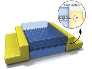
Now, a team led by Cory Dean at Columbia University appears to have cracked both these problems. The researchers developed a process to create layers of individual graphene sheets encapsulated by layers of boron nitride without using any extraneous materials, followed by exposure of the edges of the graphene sheets for electrical contact.
‘Boron nitride is, like graphene, atomically flat,’ says Dean, now based at The City College of New York. ‘When the two planar surfaces come into contact, there are extremely strong van der Waals interactions and you get powerful adhesion between them.’ So the researchers were able to use boron nitride as a ‘stamp’ to pick up, alternately, sheets of graphene and sheets of boron nitride to create a multi-layered boron nitride–graphene sandwich, without any polymer contamination.
Once the assembly has been created, a mask can be placed on the top surface and the sides plasma-etched away, rather like cutting the crusts off a sandwich. This exposes the one-dimensional edges of the graphene ‘filling’. Metal can then be deposited on these exposed edges, providing the electrical contact.
Tests showed highly efficient injection of electrons into the one-dimensional edge, and that at low temperatures electrons travel through the samples without scattering. Dean points out that the process would work with other two-dimensional materials too, such as transition metal dichalcogenides.
Peter Liljeroth, who researches graphene at Aalto University School of Science in Finland, says: ‘For graphene devices this is a fundamentally new way of making the contacts. This is the first time where researchers have succeeded in make a one-dimensional contact to a two-dimensional material.’ Liljeroth points out that while this method of polymer-free fabrication ‘sounds like a boring practical detail, it is very important for the highest performing devices ... the requirement of no polymer residue is not at all simple.’


No comments yet