
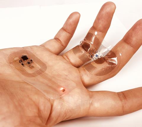
Flexible electronics that can conduct like biological tissue, degrade harmlessly in the body and interface seamlessly with organs are transforming medical devices. Anna Demming explores how researchers are unravelling the complex relationships between material structure and function to create the next generation of biocompatible technologies
- Advances in flexible and degradable electronics are enabling medical devices that better mimic biological tissues, including resorbable pacemakers and artificial retinas.
- Conductive polymers and nanoscale materials such as ultrathin silicon provide soft, stretchable and biocompatible platforms capable of transporting both ions and electrons.
- Researchers are working to unravel complex structure–function relationships in materials like conjugated polymers and hydrogels, using tools such as machine learning to optimise conductivity, stability and mechanical performance.
- Emerging applications include triggerable biodegradable devices, biocompatible OLEDs and organic artificial neurons that communicate using the same ionic signals as the body, though challenges remain in stability, manufacturability and clinical integration.
This summary was generated by AI and checked by a human editor
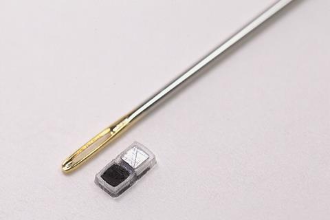
It was just millimetres in scale, completely resorbable and potentially lifesaving – in April 2025 John Rogers’ team at Northwestern University in Illinois, US, reported the latest in their series of pacemaker devices that automatically degrade into water-soluble substances that can be excreted through the kidneys once their job is complete. This one was no bigger than a grain of rice, designed to support new born babies struggling in the first few weeks of life. The work brought the notion of tissue-compatible electronics to a whole new level.
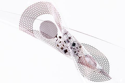
The discovery in the late 1970s that certain polymers could conduct electricity radically revised our notions of what electronics could look and feel like. While potential applications are numerous, the soft side of electronics has found particularly fertile ground for development in medicine. Electronic devices that are flexible have advantages beyond the simple ability to conform to dynamic tissue morphologies for a better fit; they can also pass for natural tissue, which avoids the launch of an immune response, scar tissue generation and ultimately rejection from the body. Further replicating the body’s ability to break down deceased cells with a degradable device is one way of taking this pursuit of electronics with biomimetic properties a step further. As well as flexing like organic tissue, many conductive polymers can conduct like the body’s natural wiring, transferring whole ions as well as electrons. This too is enabling impressive devices such as artificial retinas that can partially restore vision.
Such feats might suggest that the materials science for these devices is nailed. However, there is also greater understanding of the exacting requirements a material needs to meet if it is to enable a device that plays a useful role for the body. As well as honing the properties for possible thermal, optical, electrical or ultrasound monitoring and intervention, the mechanical demands for the required robust high-quality contact are steep. More than merely flexible, a material needs to be able to stretch, flex and fit like a second skin with high level impedance matching. ‘We struggle with that in a lot of our applications,’ Rogers tells Chemistry World.
Here, options are increasing. Already, the range of flexible materials that can be used as conductive elements in a device represents an embarrassment of riches compared to what was known in the 1970s. Even traditional silicon electronics has its place leveraging the advantages attained with diminished dimensions, while at the opposite end of the spectrum other types of materials attracting intense research might be more aptly described as electronic jelly. Nonetheless drawing a line between how a material is structured and its corresponding properties remains a dark art, one where machining learning approaches among others are beginning to shed a little light.
From conductive polymers to nanosilicon
When Alan Heeger, Alan MacDiarmid and Hideki Shirakawa completed their Nobel prizewinning work to establish the field of conductive polymers, they disrupted a lot of the traditional dichotomies of plastic insulators versus metals and semiconductors. The conjugated polymers they worked on are long molecules built up of several repeating units strung along a carbon backbone. The plastics and rubbers used to insulate conducting wires are made from a type of polymer too, but key to the conductive properties Heeger, MacDiarmid and Shirakawa identified is alternating single and double carbon–carbon bonds in the backbone. ‘That essentially leaves some ability for the polymer to move charges along its backbone or between polymer chains, allowing charge transport along the polymer,’ explains Aram Amassian, materials scientist at North Carolina State University in the US. Doping the polymer with electron donating groups or extracting ions can increase the conductivity of these ‘conjugated’ polymers by several orders of magnitude, and the mobility of those ions enables ionic as well as electronic transport.
We found that ultrathin silicon is a pretty darn good semiconductor
All this has been big news, opening the door to materials combining charge transport with a wider range of properties than was previously possible, including flexibility. But another huge materials revolution has also been underway since the 1970s as synthesis and fabrication methods have unleashed the potential of nanoscale materials, which can be very useful for medical applications. ‘Electronic components can be scaled down to small sizes, and when you do that, the performance goes up, and so the material load on the body goes down,’ Rogers explains.
What is more, it turns out that when you diminish the dimensions of a semiconductor like silicon to the nanoscale, a lot of useful electronic properties are retained while the rigid mechanical properties that once defined it go out the window. ‘We found that ultrathin silicon is a pretty darn good semiconductor,’ he adds. Silicon is also water soluble when nanosized and the solution – silicic acid – is a natural part of the daily diet, key factors when designing a device that will degrade into biologically benign products. Working with this familiar semiconductor also opens up the potential to leverage a billion-dollar silicon electronics industry infrastructure, which can be useful for scaling up device fabrication, depending on the circuit complexity.
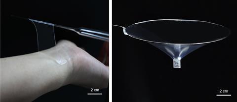
Nonetheless, pushing monitoring devices to the frontiers still poses mechanical property challenges. Almost all clinical grade measurements to monitor biomarkers require ‘an intimate skin interface, not just something that kind of conforms’, points out Rogers. ‘Once you have disrupted that skin coupling, it really has a large effect on the measurement that you’re trying to make.’ Here hydrogels are attracting a lot of interest. Naturally moist – they are mostly water – hydrogels have the chemistry to allow covalent bonding to the surfaces of tissues, and that allows robust skin coupling for measurements.
Yan Wang is an associate professor at Guangdong Technion in China, and her group focuses on developing soft wearable devices in healthcare. She notes how the skin contact improves as hydrogel thickness decreases, since the flexural rigidity drops in inverse proportion to the third power of the thickness. However, this improved contact comes with a trade-off. ‘If you make the hydrogel very thin to improve skin conformity and breathability, it usually becomes mechanically fragile,’ she explains. ‘If you make it thick enough to be robust, you lose comfort and create interfacial gaps.’ To get around this and enable ultrathin hydrogels just 2.7μm thick that are simultaneously robust, she and her colleagues used a supportive electrospun polyurethane nanomesh.
As well as the nanomesh support, Wang and her team optimised the chemistry of the hydrogel itself. They used a binary solvent mixture of water and glycerol since the glycerol helps to retain the water needed for ion mobility. They also incorporated lithium chloride to provide ions for transport and help prevent the hydrogel from freezing. The concentration required careful management as well since it could disrupt the polymer framework if too high. As Wang explains, they also tuned the network structure and mechanical behaviour – ‘properties that indirectly influence conductivity through hydration and ion mobility’ – by using vanillin as a cross-linking agent. Thus, the hydrogel design requires a careful balance of a number of interacting factors and not all of the relevant structure–function relationships have been firmly pinned down. ‘We understand the main levers, but the field still lacks fully predictive structure–property models,’ she says. ‘Especially when you consider long-term wear, temperature changes, dehydration and the skin interface.’ She is keen to establish a more complete quantitative understanding of how microstructure – network density, interactions, porosity and reinforcement architecture – maps onto conductivity and long-term signal quality under real-world use.
Unravelling structure–function relationships
Despite all the progress of the past five decades something similar could be said for conjugated polymers. Numerous experiments have shown how changing the polymer synthesis process and the doping can change the electronic and ionic properties by orders of magnitude, but what has remained more elusive is how. Amassian lists a number of candidate processes. It is possible that some approaches lead to more ordered polymers with straighter chains that are more connected and so provide a better pathway for charge transport. However, it is equally plausible that mere numbers offer the best explanation and that just adding more carriers through doping allows more charges (electrical current) to move along and thus the illusion of faster transport.
The doping process itself remains something of a mystery as it is not yet clear where the dopants nestle within the structure, whether it is right up against the polymer chains, between polymer chains or elsewhere. ‘It’s kind of been a puzzle,’ says Amassian. ‘Exactly how are these knobs influencing the important functional properties?’
Are we getting to the bottom of what is truly happening at the molecular scale
The conundrum persists despite the concerted efforts of a number of research groups to shed light on structure–function relationships in these materials. As Amassian describes, through experiments testing one hypothesis after another, the field has amassed evidence of correlations between all kinds of variables at various scales and different material properties. However, ‘when you start to put all that together, you wonder if all of these matter’, he says. ‘Are we getting to the bottom of what is truly happening at the molecular scale, and at different scales?’
In an attempt to implement a more hypothesis-agnostic approach to investigating structure–function relationships, he and his team enrolled a machine learning algorithm to design experiments that would explore as much of the potential structure–function parameter space as possible. The algorithm also had a Bayesian element to it so that while the project is hypothesis-agnostic at the outset, the direction of each subsequent experiment is influenced by the results accrued on the way. An analogy might be someone clearing up a jar of beads they have knocked over – if they find a bead under the couch they will likely then look more closely under the couch for other beads than the rest of the room.
This kind of Bayesian optimisation helps whittle the infinity of possible experiments within the project scope down to a more manageable set of experiments that are focused around the parameter space combining least knowledge with the most promising results as knowledge is accrued, such as regions harbouring both a lot of uncertainty and evidence of good conductivity.
![Chemical structures of PBTTT (Poly(2,5-bis(3-alkylthiophen-2-yl)thieno[3,2-b]thiophene)) and TCNQ (Tetracyanoquinodimethane)](https://d2cbg94ubxgsnp.cloudfront.net/Pictures/web/e/z/k/flex_534085.svgz)
Amassian and his colleagues focused their investigation on a conjugated thiophene polymer PBTTT doped with electron-accepting cyanocarbon F4TCNQ. In particular they focused on the localisation and mobility of the resulting polarons – quasiparticles used to describe interactions between charges and the dynamics of a crystal lattice. Some of their results further endorsed existing ideas, such as evidence linking polymer order and the alignment of layers with the conductivity. However, others came as a surprise.
The polymer PBTTT has crystalline and amorphous regions and what they found was that in the samples with highest conductivity, the dopants were at the periphery of the crystalline regions, which puzzled them as it is the crystalline regions that are expected to be responsible for the conductive properties. ‘How could we have dopants outside the crystalline region of the polymer and still have something very conducting?’ asks Amassian. ‘It just didn’t add up immediately.’ Theoretical follow-up calculations helped the team to figure out that if the dopant were more centrally embedded in the crystalline regions it was actually more pinned by the counterions in the polymer crystal and less mobile as a result. ‘The further out it is – it still interacts – but it creates this delocalized charge that can glide along the polymer much more easily,’ says Amassian.
Clinical applications
Understanding these structure–function relationships a little better could help design materials for functional devices in high demand for medical systems, such as biocompatible OLEDs, something John Rogers expresses great interest in. At the moment the automatically degradable pacemakers his group have developed work through a coating that protects the pacemaker from degrading until a certain period has passed during which the coating slowly dissolves. However, as he puts it, this means you have to start the clock as soon as the pacemaker is in place. OLEDs might be one way of triggering degradation once the device is already inside, so that it can stay completely intact until triggered. Other OLED medical functions include optical measurements, such as blood oxygenation, and neural modulation. ‘Optical function is something that’s missing, and it would be really valuable to add that to the toolbox of device options in this space,’ says Rogers, adding that it will likely ‘require some new chemistry’.
Artificial neurons are another direction for medical device development, and one that Amassian’s group is collaborating on with Paschalis Gkoupidenis’ group at North Carolina State University. Amassian’s fascination with conjugated polymers stems in large part from the way they can combine electronic transport like that in traditional electronics with the transport of ions that the body uses for signalling. ‘Those two worlds – they don’t really use the same language for communication,’ he says. Thus the organic artificial neurons they are looking into based on conjugated polymers have the special quality of using ‘the same communication modes, the ions, the neurotransmitters’ as biology. ‘No other technology has been shown to do that,’ he adds.
Understanding which parts of the polymer the ions interact with has important parallels with understanding how doping influences polaron formation. The action of ions on changing the electronic transport properties means these materials behave like mixed ionic–electronic conductors (MIECs). In medicine, as well as advances in artificial retinas using this kind of artificial neuron, research groups including that of George Malliaras at Cambridge University in the UK are looking at using conjugated polymers that behave like MIECs to monitor neural activity. This could be used to forecast a seizure and possibly launch an intervention to prevent it, but its use cases may be far more wide ranging. Amassian’s group has worked with the Malliaras lab and, as Amassian sees it, a key value proposition of MIEC polymers is that they swell in biological media, enabling artificial neurons and other devices to receive the full biological signal within all polymer chains within its volume, obviating detection issues around surface atoms in rigid materials.
Organic artificial neurons may also inform the design of more efficient computation and communication devices, taking something of the efficiency achieved in the human brain, which typically runs on just around 20W of power. With traditional electronics, ‘you would need megawatts of power, and it would be a billion dollar facility, just to be able to do what our brain does’, he adds. ‘Which is one of the reasons why data centres require so much electricity’.
Despite all the progress, substantial challenges remain for the further development of artificial neurons as well as other medical electronic materials into functional devices. One is how to stabilise the materials, which can require combining properties that often conflict. Water-resistant hydrogels still need to allow ions to permeate but not swell or come off in the shower.
The leap from raw material to something that a clinic can use is also an issue for everyone working on conductive materials for clinical use. ‘You open up a box, there’s an instruction manual, there’s a spec sheet,’ says Rogers describing the format needed for clinical use. ‘It’s a whole different world compared to what is typically possible in an academic laboratory environment.’ All this requires what amounts to low level manufacturing facilities. ‘I think until you’ve done that, you don’t have a good sense of how the technology is going to fit into the clinical workflow.’ This is unfortunate, he says, since most academic labs do not have the capacity to deliver devices to clinical collaborators at the necessary technology readiness level for them to use and evaluate. ‘The result is a gap that one must work very hard to overcome.’ Nevertheless, with a positive track record in the field to motivate them, these are challenges that researchers at the vanguard of materials design and device development seem excited to see through.
Anna Demming is a science writer based in Bristol, UK


No comments yet