Metallic nanostructures fashioned by precise electrodeposition
A pen that performs 3D printing on the nanoscale has been developed by scientists in South Korea.
The pen, created by Seongpil Hwang of Korea University and co-workers, amalgamates the precision of atomic force microscopy with a diffusion limited current from a microscopic electrode.
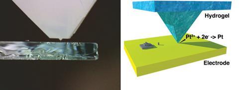
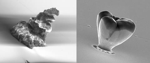
At its tip, the pen has a microscopic hydrogel pyramid, the sharp apex of which is soaked in an electrolyte for electrochemical reactions. A nanometre-scale area for reactant mass transport results from contact between this tip and an ultramicroelectrode. Controlling this contact with a nanopositioning system regulates a faradaic reaction that enables electroplating to give precise nanostructures; in this case 3D structures of platinum were deposited on a gold electrode – some with dimensions less than 100nm.
‘To the best of our knowledge, our hydrogel pen is the first example of a 3D printing pen,’ explains Hwang. ‘However, we were motivated by three techniques: dip-pen lithography developed by Chad Mirkin of Northwestern University [US], nanopipettes built by Patrick Unwin at the University of Warwick [UK] and micro-nozzels developed by Jennifer Lewis from Harvard University [US].’
‘3D additive nanomanufacturing is the next frontier for rapid prototyping of nanoscale components,’ comments materials scientist Harish Bhaskaran from the University of Oxford, UK. ‘There are many challenges at these scales and control of features, the reliability of these pens in the long-term, etc, will all play a role in their adoption in products in the future. However, this is an important first step and quite interesting because the technique is scalable.’
References
This article is free until 13 January 2015. Download it here:
H Kang, S Hwang and J Kwak, Nanoscale, 2015, DOI: 10.1039/c4nr06041e


No comments yet